


 Happy’s Tech Talk #44: Memories of the ‘Mystery Systems of the East’
 The Right Approach: Electro-Tek—A Williams Family Legacy, Part 2
 Alpha Insights, Performance by Design: Understanding Heat at the Core of Every Design


Building Miniature Optical Antennas Using DNA as a Guide
February 5, 2018 | University of JyväskyläEstimated reading time: 2 minutes
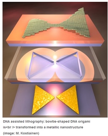
A new fabrication technique combines programmable DNA origami shapes and conventional lithography methods to create metallic nanoantennas and chiral shapes for diverse applications.
Research groups from University of Jyväskylä and Aalto University (Finland) together with researchers from California Institute of Technology (Caltech, USA) and Aarhus University (iNANO Center, Denmark) have reported a new highly parallel technique to fabricate precise metallic nanostructures with designed plasmonic properties by means of different self-assembled DNA origami shapes. The so-called DALI (DNA-assisted lithography) method has been published in the latest issue of Science Advances.
“We can build virtually any nanoscale shape using a DNA origami technique, and now we have shown how to use these accurate shapes as “stencils” to create millions of fully metallic nanostructures with 10 nm feature sizes in one go”, explains Adjunct Professor Veikko Linko from Aalto University. The trick in the DALI method is that when the DNA structures are deposited on a chip coated with silicon, silicon oxide can be selectively grown only on the bare areas of the substrate. “By controlling this process, we can create origami-shaped openings on the grown silicon oxide layer, and this layer can be used as a mask for the following lithography steps. Finally, we evaporate metal through these openings and create metallic structures having the same shape and size as the original DNA origami on a transparent substrate, such as sapphire”, Boxuan Shen from the Nanoscience Center of University of Jyväskylä describes the method.
The tiny metallic features cover the whole transparent substrate, and therefore these surfaces have intriguing optical properties. The small dimensions of the structures – in the range of ten nanometers – allow further tuning of these properties at the visible wavelength range. “Actually, we have demonstrated here a structure that we believe is the world’s smallest entirely metallic bowtie-shaped antenna. This extremely small size extends the operating range of optical features from infrared to visible”, states Adjunct Professor Jussi Toppari from Molecular Electronics and Plasmonics group at University of Jyväskylä. These antennas can find use in dozens of optical and plasmonic applications, such as surface enhanced Raman spectroscopy, biosensing or fluorescence enhancement. Moreover, the researchers demonstrated that the surfaces can be used as polarizers by fabricating chiral structures using DALI.
“The DALI method is highly parallel, and it could further enable cheap wafer-scale production of surfaces as it does not rely on costly patterning methods. It is also equipped for the future studies to provide bioinspired surfaces and metamaterials if the customized origami structures can be arranged on the substrate before metallization”, envisions Professor Mauri Kostiainen from the Biohybrid Materials Group at Aalto University.
Share on:


Testimonial
"Your magazines are a great platform for people to exchange knowledge. Thank you for the work that you do."
Simon Khesin - Schmoll MaschinenSuggested Items
Zhen Ding Reports Solid Performance for the First Three Quarters of 2025
11/13/2025 | Zhen DingZhen Ding Technology Holding Limited, a global leading PCB manufacturer, announced its consolidated financial results for the third quarter of 2025.
LPKF Delivers Key Strategic Technology to Fraunhofer's Glass Panel Technology Group
10/29/2025 | LPKFLPKF Laser & Electronics SE is one of the initiators of the Glass Panel Technology Group (GPTG), a consortium encompassing the entire process chain for advanced semiconductor packaging with glass substrates.
MKS’ Atotech Showcases Next-gen PCB and Substrate Manufacturing Solutions at CPCA Plus 2025
10/24/2025 | MKS Inc.MKS Inc., a global provider of enabling technologies that transform our world, announced its participation in CPCA Plus Show 2025, taking place October 28 – 30 at Shenzhen International Convention and Exhibition Center.
Zhen Ding Highlights AI PCBs, IC Substrates at TPCA 2025
10/22/2025 | Zhen DingThe annual PCB industry event, TPCA Show 2025, kicked off on October 22 at the Nangang Exhibition Center. Zhen Ding Tech Group showcased a full range of high-end PCBs and IC substrates under the theme of artificial intelligence (AI).
MKS’ Atotech, ESI to Participate in TPCA Show & IMPACT Conference 2025
10/17/2025 | MKS’ AtotechMKS Inc., a global provider of enabling technologies that transform our world, announced that its strategic brands Atotech (process chemicals, equipment, software, and services) and ESI (laser systems) will showcase their latest range of leading manufacturing solutions for printed circuit board (PCB) and package substrate manufacturing at the upcoming 26th TPCA Show 2025 to be held at the Taipei Nangang Exhibition Center from 22-24 October 2025.