


 The Chemical Connection: Onshoring PCB Production—Daunting but Certainly Possible
 It’s Only Common Sense: The Phone Is Still Mightier Than the Keyboard


Engineers on a Roll Toward Smaller, More Efficient Radio Frequency Transformers
May 15, 2018 | University of Illinois at Urbana-ChampaignEstimated reading time: 2 minutes
The future of electronic devices lies partly within the "internet of things" - the network of devices, vehicles and appliances embedded within electronics to enable connectivity and data exchange. University of Illinois engineers are helping realize this future by minimizing the size of one notoriously large element of integrated circuits used for wireless communication - the transformer.
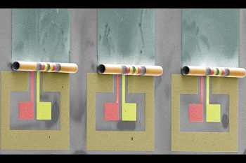
Three-dimensional rolled-up radio frequency transformers take 10 to 100 times less space, perform better when the power transfer ratio increases and have a simpler fabrication process than their 2-D progenitors, according to a paper detailing their design and performance in the journal Nature Electronics.
"Transformers are one of the largest and heaviest elements on any circuit board," said principal investigator Xiuling Li, a professor of electrical and computer engineering. "When you pick up an LED light bulb, it feels heavy for its size and that is in part because of the bulky transformer inside. The size of these transformers may become a key obstacle to overcome in the future for wireless communication and IoT."
Transformers use coiled wires to convert input signals to specific output signals for use in devices like microchips. Previous researchers have developed some radio frequency transformers using a stacked conducting material to solve the space problem, but these have limited performance potential. This limited performance is due to inefficient magnetic coupling between coils when they have a high turns ratio, meaning that the primary coil is much longer than the secondary coil, or vice versa, Li said. These stacked transformers need to be made using special materials and are difficult to fabricate, bulky and unbendable - things that are far from ideal for internet of things devices.
The new transformer design uses techniques Li's group previously developed for making rolled inductors. "We are making 3-D structures using 2-D processing," Li said. The team deposits carefully patterned metal wires onto stretched 2-D thin films. Once they release the tension, the 2-D films self-roll into tiny tubes, allowing the primary and secondary wires to coil and nest perfectly inside each other into a much smaller area for optimum magnetic induction and coupling.
The nested 3-D architecture leads to high turns ratio coils, Li said. "A high turns ratio transformer can be used as an impedance transformer to improve the sensitivity of extremely low power receivers, which are expected to be a key enabler for IoT wireless front ends," said electrical and computer engineering professor and co-author Songbin Gong.
Rolled transformers can also receive and process higher frequency signals than the larger devices.
"Wireless communication will be faster and use higher-frequency signals in the future. The current generation of radio frequency transformers simply cannot keep up with the miniaturization requirements and high-frequency operation of the future," said lead author and postdoctoral researcher Wen Huang. "Smaller transformers with more turns allow for better reception of faster, high-frequency wireless signals, as well as high-level integration in IoT applications."
The new transformers have a robust fabrication process - stable beyond standard foundry temperatures and compatible with industry-standard materials. This study used gold wire, but the team has successfully demonstrated the fabrication of their rolled devices using industry-standard copper.
"The next step will be to use thinner and more-conductive metal such as graphene, allowing these devices to be made even smaller and more flexible. This advancement may make it possible for the devices to be woven into the fabrics of high-tech wearables," Li said.
Share on:


Testimonial
"Your magazines are a great platform for people to exchange knowledge. Thank you for the work that you do."
Simon Khesin - Schmoll MaschinenSuggested Items
Episode 6 of Ultra HDI Podcast Series Explores Copper-filled Microvias in Advanced PCB Design and Fabrication
10/15/2025 | I-Connect007I-Connect007 has released Episode 6 of its acclaimed On the Line with... American Standard Circuits: Ultra High Density Interconnect (UHDI) podcast series. In this episode, “Copper Filling of Vias,” host Nolan Johnson once again welcomes John Johnson, Director of Quality and Advanced Technology at American Standard Circuits, for a deep dive into the pros and cons of copper plating microvias—from both the fabricator’s and designer’s perspectives.
Nolan’s Notes: Tariffs, Technologies, and Optimization
10/01/2025 | Nolan Johnson -- Column: Nolan's NotesLast month, SMT007 Magazine spotlighted India, and boy, did we pick a good time to do so. Tariff and trade news involving India was breaking like a storm surge. The U.S. tariffs shifted India from one of the most favorable trade agreements to the least favorable. Electronics continue to be exempt for the time being, but lest you think that we’re free and clear because we manufacture electronics, steel and aluminum are specifically called out at the 50% tariff levels.
MacDermid Alpha & Graphic PLC Lead UK’s First Horizontal Electroless Copper Installation
09/30/2025 | MacDermid Alpha & Graphic PLCMacDermid Alpha Electronics Solutions, a leading supplier of integrated materials and chemistries to the electronics industry, is proud to support Graphic PLC, a Somacis company, with the installation of the first horizontal electroless copper metallization process in the UK.
Electrodeposited Copper Foils Market to Grow by $11.7 Billion Over 2025-2032
09/18/2025 | Globe NewswireThe global electrodeposited copper foils market is poised for dynamic growth, driven by the rising adoption in advanced electronics and renewable energy storage solutions.
MacDermid Alpha Showcases Advanced Interconnect Solutions at PCIM Asia 2025
09/18/2025 | MacDermid Alpha Electronics SolutionsMacDermid Alpha Electronic Solutions, a global leader in materials for power electronics and semiconductor assembly, will showcase its latest interconnect innovations in electronic interconnect materials at PCIM Asia 2025, held from September 24 to 26 at the Shanghai New International Expo Centre, Booth N5-E30