


 The Marketing Minute: If Your Marketing Budget Gets Cut in Half, Then What?
 Punching Out: How Are the Big Boys in Electronics Doing?
 It’s Only Common Sense: Complexity Is the Enemy of Profit


Groundbreaking Method Creates Better and Cheaper Nanochips
March 18, 2019 | CORDISEstimated reading time: 2 minutes
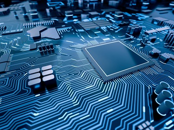
Technology has advanced by leaps and bounds since the first computers that took up entire rooms and weighed many tonnes. In the decades that followed, computers and electronic components have become increasingly smaller, faster and more energy-efficient. This ongoing technological progression towards more diminutive and more powerful computers brings us to today, where advances are sought at the nanoscale.
A team of researchers supported by the EU-funded project SWING have now achieved another breakthrough in nanoscale technology. They’ve invented a new way to fabricate atom-thin processors on 2D semiconductors. Their discovery could radically affect semiconductor research using 2D materials and bring about profound changes in the field of nanoscale chip production. The team led by New York University Tandon School of Engineering Professor of Chemical and Biomolecular Engineering Elisa Riedo discuss their results in a paper published in the journal ‘Nature Electronics’.
The researchers’ innovative method involves lithography using a probe heated above 100 °C. Referred to as thermal scanning probe lithography (t-SPL), this technique performed better than the usual methods for fabricating metal electrodes on 2D semiconductors such as molybdenum disulfide (MoS2). Materials such as MoS2 are considered promising for the development of novel electronic components.
The Method’s Advantages
According to the study, the t-SPL method outperforms electron beam lithography (EBL) – the method currently in use—in a number of ways. First, it greatly improves the quality of the 2D transistors. It does this by counteracting the Schottky barrier, which stops the flow of electrons where the semiconductor material and the metal meet. Second, it makes it easier for chip designers to image the 2D semiconductor and pattern the electrodes in any way they wish—something the EBL method doesn’t allow. Third, the t-SPL method promises substantial savings not only in initial investment costs but also in operating costs. Since such a system operates in ambient conditions, it consumes much less power and therefore doesn’t need to generate high-energy electrons or an ultra-high vacuum. Finally, nanochip production on an industrial scale is easily achieved with this new fabrication method using parallel thermal probes.
An article published on the ‘Science Daily’ website reports Prof. Riedo’s hope that t-SPL will move most fabrication out of clean rooms which are expensive and in short supply and into individual laboratories. If this is made possible it might lead to more rapid advances in materials science and chip design than currently achieved.
Since its launch in 2016, SWING (Patterning Spin-Wave reconfIgurable Nanodevices for loGics and computing.) has focused on pushing forward the field of magnonics—a rapidly growing field combining magnetism, spintronics and electronics. SWING’s interdisciplinary approach has benefited from expertise in magnetism, nanoscience, photonics and entrepreneurship. The project ends in October 2019.
Share on:


Subscribe
Stay ahead of the technologies shaping the future of electronics with our latest newsletter, Advanced Electronics Packaging Digest. Get expert insights on advanced packaging, materials, and system-level innovation, delivered straight to your inbox.
Subscribe now to stay informed, competitive, and connected.
Suggested Items
Quantum Benchmarking Initiative Expands Quest to Separate Hype from Reality
03/18/2026 | DARPAAs the quantum computing field accelerates, DARPA’s Quantum Benchmarking Initiative (QBI) is expanding to capture its momentum.
Meet the Author Podcast: Martyn Gaudion Unpacks the Secrets of High-Speed PCB Design
07/16/2025 | I-Connect007In this special Meet the Author episode of the On the Line with… podcast, Nolan Johnson sits down with Martyn Gaudion, signal integrity expert, managing director of Polar Instruments, and three-time author in I-Connect007’s popular The Printed Circuit Designer’s Guide to... series.
Intervala Hosts Employee Car and Motorcycle Show, Benefit Nonprofits
08/27/2024 | IntervalaIntervala hosted an employee car and motorcycle show, aptly named the Vala-Cruise and it was a roaring success! Employees had the chance to show off their prized wheels, and it was incredible to see the variety and passion on display.
KIC Honored with IPC Recognition for 25 Years of Membership and Contributions to Electronics Manufacturing Industry
06/24/2024 | KICKIC, a renowned pioneer in thermal process and temperature measurement solutions for electronics manufacturing, is proud to announce that it has been recognized by IPC for 25 years of membership and significant contributions to electronics manufacturing.
Boeing Starliner Spacecraft Completes Successful Crewed Docking with International Space Station
06/07/2024 | BoeingNASA astronauts Barry "Butch" Wilmore and Sunita "Suni" Williams successfully docked Boeing's Starliner spacecraft to the International Space Station (ISS), about 26 hours after launching from Cape Canaveral Space Force Station.