


 Happy’s Tech Talk #44: Memories of the ‘Mystery Systems of the East’
 The Right Approach: Electro-Tek—A Williams Family Legacy, Part 2
 Alpha Insights, Performance by Design: Understanding Heat at the Core of Every Design


Toray Creates Revolutionary PPS Film for 5G Circuit Boards
December 23, 2019 | Toray IndustriesEstimated reading time: 2 minutes
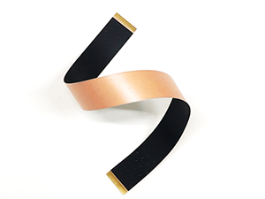
Toray Industries, Inc., announced that it has created a polyphenylene sulfide (PPS) film that maintains the outstanding dielectric characteristics—or low dielectric losses of electrical energy—flame retardancy, and chemical robustness of that polymer while remaining thermally resistant at 40°C higher than conventional counterparts. The new film resists deformation and is dimensionally stable near its melting point. PPS is a super engineering plastic that also offers excellent electrical insulation. It is crystalline, with a melting point of 280°C.
Employing the new film in flexible printed circuits offering 5G and other fast data rates would offer two key benefits. First, the film would cut the transmission losses of communication devices at high frequencies. Second, it would help stabilize high-speed communication across the temperature and humidity spectrums. Flexible printed circuits are film-like wiring boards in which electrical circuits are formed on base materials from bonding thin, soft insulating base films with copper foil or other conductive metals.
Toray has already completed the technology for the new film on a pilot basis, and looks to have a mass production setup in place during fiscal 2020 that would help swiftly popularize devices in the fast-expanding 5G arena. 5G is commanding attention as an advanced platform for delivering outstanding speed capacity, multi-connectivity, and low latency. It harnesses frequency bands below 6 GHz and above 20 GHz.
Development efforts have seen the emergence of practical liquid crystal polymer (LCP) films as flexible printed circuit substrate materials needed for 5G. The dielectric properties of such films reduce transmission losses in high-frequency bands. These films also offer thermal resistance when soldering circuit boards. The expense and processing issues of LCP films fueled the exploration of other materials that could overcome those shortcomings.
Generally PPS film offers superior flame retardancy and chemical resistance while matching or exceeding the dielectric properties of LCP film, and is far less vulnerable to temperature and humidity extremes. On the downside, PPS film deforms easily at high temperatures and provides insufficient resistance to heat when soldering circuit boards.
These considerations drove Toray to blaze a new trail in film design. It was in the course of that effort that it developed a proprietary technology that controls the crystal structure of PPS films. It thereby maintained the outstanding properties of PPS polymer while dramatically increasing thermal resistance.
Testing to 250°C confirmed that Toray’s new PPS film does not deform. Increasing thermal resistance should make it possible to employ existing processing facilities of circuit boards. Toray attained a low coefficient of thermal expansion in the thickness direction of 98 ppm/°C by employing technology it has amassed over many years to control the orientation of film molecular chains. The diverse applications that leveraging those features, including 5G transmission cables and antennas, should enable the design of smaller, multi-layered circuit boards.
By taking advantage of the high thermal dimensional stability and cost-competitiveness of TORELINA, its biaxially-oriented PPS film, Toray looks to secure the adoption of its new film in the FPC market, particularly for smartphones, and thereafter cultivate diverse applications, including for vehicular usage and base stations. In so doing, the company will create new value in keeping with its corporate philosophy of contributing to society through innovative ideas, technologies, and products.
Share on:


Testimonial
"Your magazines are a great platform for people to exchange knowledge. Thank you for the work that you do."
Simon Khesin - Schmoll MaschinenSuggested Items
The Impact of the AI Boom on PCB and Raw Materials Supply Chains
11/13/2025 | Mark Goodwin, Ventec International GroupThe PCB industry is entering a period of unprecedented structural change, driven by the demands of artificial intelligence and advanced computing. What was once a cyclical market has become a capacity race. It’s one that rewards foresight, collaboration, and strategic supply partnerships. Understanding these dynamics is essential for maintaining stability and growth across all market segments. This report, created by Ventec International Group, provides a clear view of how AI-driven demand is reshaping the PCB materials landscape and what actions are required to secure long-term supply.
Elementary, Mr. Watson: The Four Horsemen of Copper Confusion
11/12/2025 | John Watson -- Column: Elementary, Mr. WatsonIf there were a PCB Design Dictionary of Confusing Terms, the cover would feature four words that have baffled generations of engineers: polygons, pours, planes, and floods—or what I refer to as the four horsemen of copper confusion. They sound simple, as if they belong in a geometry textbook or a weather report, but in PCB design, they overlap, develop, and sound interchangeable until you realize they aren't.
Alpha Insights, Performance by Design: Understanding Heat at the Core of Every Design
11/11/2025 | Team Alpha -- Column: Alpha Insights: Performance by DesignPower isn’t just about current. It’s about control. As electronic systems grow smaller and faster, every amp and every layer generates a new source of heat. That heat is more than a byproduct. It’s a measure of efficiency, a benchmark of performance, and often the first indication of failure.
The Shaughnessy Report: Zee Plane! Zee Plane!
11/11/2025 | Andy Shaughnessy -- Column: The Shaughnessy ReportPlanes aren’t magic, but they are big time-savers. Without planes, designers would have to create thousands of traces to accomplish the same objectives. You can imagine the first time a designer thought about using a sheet of copper, asking, “Hey, why am I killing myself laying out all these traces? Can’t I just use this sheet of copper instead?”
November 2025 Design007 Magazine: Proper Plane Design
11/10/2025 | I-Connect007 Editorial TeamWithout planes, designers would have to create thousands of traces to accomplish the same objectives. Power planes provide low impedance and stable power to every component on the board, much like a large power bus. Ground planes stabilize reference voltage, improve thermal performance, and help preclude EMI issues. Power and ground plane design is often a battle of tradeoffs.