


 It’s Only Common Sense: If You’re Not Differentiated, You’re Dead
 Alpha Insights, Performance by Design: The Future of PCB Manufacturing in the Midwest
 Happy’s Tech Talk #43: Engineering Statistics Training With Free Software


Averatek Releases New High-Density Process Details at IPC APEX EXPO 2020
January 17, 2020 | AveratekEstimated reading time: 1 minute
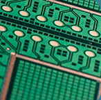
Averatek Incorporated has announced their participation in this year’s IPC APEX EXPO Conference and Exposition being held February 4th − 6th, at the San Diego Convention Center. Averatek will be presenting advanced PCB manufacturing technology as well as sharing expertise and experience in its deployment.
Averatek will first present on Tuesday, February 4th, at the technical conference followed by participation in a panel discussion at the Sessions at the Intersection. This discussion will be open to all attendees. On Wednesday, February 5th, Averatek will present at the inaugural community of interest meeting focused on additive PCB processes capable of feature sizes of 25 microns and below, exploring both the needs of next generation electronics and the needs of PCB fabricators licensing this technology.
“The electronics industry is at an inflection point.” said Haris Basit, CEO of Averatek, “Increasingly complex electronics continue to challenge traditional fabrication processes. Averatek’s A-SAP™ process resets the technology curve and opens up design opportunities that were previously unavailable.”
“We are excited to participate in this year’s IPC APEX EXPO. There is a lot to learn when working with a new, emerging technology. This IPC conference provides the opportunity to meet with, listen to and educate OEM’s, PCB Fabricators, and EMS companies all in one location. We have just scratched the surface on the ways A-SAP™ can be utilized in design and we are looking forward to insightful discussion and feedback”, said Mike Vinson, President and COO of Averatek.
Averatek’s A-SAP™ is an advanced manufacturing process for printed circuit board fabrication with trace and space as narrow as 15 microns. This process can dramatically reduce the space and weight of electronics systems, provide significant RF benefits and can be easily integrated with today’s traditional PCB manufacturing processes and materials.
About Averatek
Averatek Corporation develops and licenses advanced manufacturing processes for a variety of electronic products including very high density printed circuit boards, semiconductor packaging and RF and millimeter wave passive components. In addition, Averatek develops and sells the key chemistry that enables these advanced manufacturing processes. For more information visit www.averatek.com
Share on:


Testimonial
"We’re proud to call I-Connect007 a trusted partner. Their innovative approach and industry insight made our podcast collaboration a success by connecting us with the right audience and delivering real results."
Julia McCaffrey - NCAB GroupSuggested Items
Imec Launches 300mm GaN Program to Develop Advanced Power Devices and Reduce Manufacturing Costs
10/13/2025 | ImecImec, a world-leading research and innovation hub in nanoelectronics and digital technologies, welcomes AIXTRON, GlobalFoundries, KLA Corporation, Synopsys, and Veeco as first partners in its 300mm gallium-nitride (GaN) open innovation program track for low- and high-voltage power electronics applications.
NEDME Returns October 22 — The Northwest’s Premier Design & Manufacturing Expo
10/13/2025 | NEDMEThe Northwest Electronics Design & Manufacturing Expo (NEDME) returns on Wednesday, October 22, 2025, at Wingspan Event & Conference Center, Hillsboro. The event brings together engineers, product designers, manufacturers, educators, and community partners for a full day of industry connection, learning, and networking.
Critical Minerals: The New Power Play in Global Trade
10/13/2025 | Marcy LaRont, I-Connect007Access to critical minerals essential for electronics manufacturing, and China’s monopoly of them, is increasingly under scrutiny, with gallium (Ga) and germanium (Ge)at the forefront of this discourse. However, all critical minerals imported from China share a similar narrative, and understanding the implications of this dependency and the risks to both U.S. commercial and defense sectors has created an urgent need for a comprehensive electronics strategy to secure and diversify access to these vital minerals. In this candid interview, USPAE Executive Director Jim Will discusses the issues and the mitigation steps that must be taken to adequately address them.
Precision PCB Acquires Assets of Microplace
10/13/2025 | Precision Technologies Inc.Precision Technologies Inc., doing business as Precision PCB, a One-Stop PCB Fabrication and Assembly services company with 27 years of experience providing Quality, Reliability and Excellence in customer service, has acquired the assets of Microplace, Inc.
Electronics U Expands Global Workforce Training for the Electronics Industry
10/13/2025 | Global Electronics AssociationThe Global Electronics Association unveiled Electronics U, the new name and expanded vision for its workforce training and certification platform.