


 It’s Only Common Sense: Marketing Isn’t Fluff, It’s Ammunition
 Driving Innovation: Mechanical and Optical Processes During Rigid-flex Production
 The Chemical Connection: Onshoring PCB Production—Daunting but Certainly Possible


HENSOLDT and Nano Dimension Achieve Breakthrough in Electronics 3D Printing
May 19, 2020 | Nano DimensionEstimated reading time: 1 minute
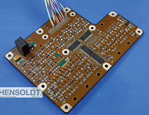
Sensor solutions provider HENSOLDT together with the leading Additively Manufactured Electronics (AME)/Printed Electronics (PE) provider, Nano Dimension, has achieved a major breakthrough on its way to utilizing 3D printing in the development process of high-performance electronics components. Utilizing a newly developed dielectric polymer ink and conductive ink from Nano Dimension, HENSOLDT succeeded in assembling the world-wide first 10-layer printed circuit board (PCB) which carries high-performance electronic structures soldered to both outer sides. Until now, 3D-printed boards could not bear the soldering process necessary for two-sided population of components.
“Military sensor solutions require performance and reliability levels far above those of commercial components.” said HENSOLDT CEO, Thomas Müller. “To have high-density components quickly available with reduced effort by means of 3D printing gives us a competitive edge in the development process of such high-end electronic systems.”
“Nano Dimension’s relationship with HENSOLDT is the type of partnership with customers we are striving for,” commented Yoav Stern, Nano Dimension President and CEO. “Working together and learning from HENSOLDT led us to reach a first-of-its-kind in-depth knowledge of polymer materials applications. Additionally, it guided us in the development of Hi-PEDs (high performance electronic device) that create competitive edges by enabling unique implementations with shortest time to market.”
AMEs are useful to verify a new design and functionality of specialized electronic components before production. AME is a highly agile and individual engineering methodology to prototype a new electronic circuitry. This leads to significant reduction of time and cost in the development process. Furthermore, AME gives a verified and approved design before production starts, leading to higher quality of the final product.
HENSOLDT started working with Nano Dimension’s DragonFly 3D printing system in 2016, in order to examine the possibilities of 3D printing electronics. Last year, HENSOLDT successfully implemented the DragonFly Lights-Out Digital Manufacturing (LDM) printing technology, the industry’s only additive manufacturing platform for round-the-clock 3D printing of electronic circuitry.
Share on:


Testimonial
"In a year when every marketing dollar mattered, I chose to keep I-Connect007 in our 2025 plan. Their commitment to high-quality, insightful content aligns with Koh Young’s values and helps readers navigate a changing industry. "
Brent Fischthal - Koh YoungSuggested Items
Electronics Manufacturing Powers U.S. Growth, Supporting 5.2 Million Jobs and $1.8 Trillion in Output
11/03/2025 | Global Electronics AssociationNew report from Global Electronics Association shows electronics industry contributes $853 billion to GDP and delivers average annual wages exceeding $156,000, reinforcing its role as a pillar of U.S. economic resilience.
Infinite Electronics, RS Group Expand Partnership to Deliver L-com Connectivity Solutions to European and APAC Markets
11/03/2025 | PRNewswireL-com, an Infinite Electronics brand and a supplier of wired and wireless connectivity products, has expanded their strategic cooperation agreement with RS Group, a U.K.-based global provider of products and services for industrial customers, to begin distributing L-com products across European and APAC markets via the RS Group website.
DuPont Completes Separation of Qnity Electronics
11/03/2025 | PRNewswireDuPont announced that it completed the separation of its electronics business into an independent public company, Qnity Electronics, Inc., on November 1, 2025.
TTM Technologies Receives Two Awards from the Global Electronics Association at the 2025 IPC CEMAC Conference
11/03/2025 | Globe NewswireTTM Technologies, Inc. announced that two of its team members received prestigious Asia Steering Committee Outstanding Service Awards from the Global Electronics Association (formerly named IPC connecting global electronics industry) at the 2025 IPC CEMAC Electronics Manufacturing Annual Conference in Shanghai.
Ethiopian Airlines Selects Cassiopée Alpha from Safran for Fleet-wide Flight Data Monitoring
11/03/2025 | SafranSafran Electronics & Defense is proud to announce that Ethiopian Airlines has selected Cassiopée Alpha, its advanced flight data analysis platform, to optimize and secure operations across the airline’s entire fleet of 147 aircraft, including Airbus A350, Boeing 787, and Boeing 737 MAX models.