


 It’s Only Common Sense: Your Biggest Competitor Is Complacency
 The Chemical Connection: Onshoring PCB Production—Daunting but Certainly Possible
 Marcy’s Musings: The Legislative Outlook—Helping or Hurting?


MKS Sees Strong Early Market Adoption in Asia for its Newest HDI PCB Laser Manufacturing Solution
September 2, 2020 | MKS Instruments, Inc.Estimated reading time: 2 minutes
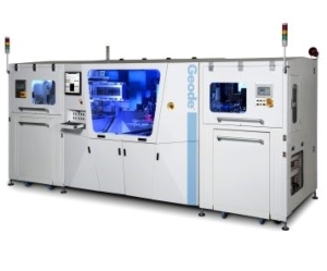
MKS Instruments, Inc., a global provider of technologies that enable advanced processes and improve productivity, announced that Meiko Electronics Co. Japan has purchased multiple ESI® Geode™ Systems to enhance its high-volume HDI PCB manufacturing capability. The recently released CO2-laser-based systems will be deployed at Meiko’s high-end manufacturing facility in Vietnam.
“We are pleased with the market adoption of the Geode system,” said MKS President and CEO John T.C. Lee. “Geode is well-positioned to take advantage of the growing market for HDI PCB processing solutions, as electronics manufacturers continue the path of miniaturization in order to meet the demand for smaller and more capable devices.”
The Geode system delivers many benefits for high-end applications, such as 5G. According to Atsushi Sakate, Executive Officer, General Manager of Production at Meiko,
“Beyond the Geode system’s higher drilling throughput and accuracy, the system’s smaller footprint and lighter weight enables us to plan capacity expansion with much more flexibility. Add to this the broad range of applications and materials that Geode can process, and the decision is clear.”
Developed by MKS’ Equipment & Solutions Division, already a market leader in flex PCB laser drilling solutions, the Geode system is optimized to process the rigid HDI PCBs and package substrates widely used in consumer electronics, such as smartphones and other handheld devices. Building on MKS’ technology leadership in laser processing for flexible printed circuits, Geode’s new CO2 laser technology and control capabilities deliver breakthrough performance. Its superior throughput, refined power control and small system footprint meet the needs of high-volume PCB manufacturers. Learn more about the ESI Geode System at www.esi.com.
About MKS Instruments
MKS Instruments, Inc. is a global provider of instruments, systems, subsystems and process control solutions that measure, monitor, deliver, analyze, power and control critical parameters of advanced manufacturing processes to improve process performance and productivity for our customers. Our products are derived from our core competencies in pressure measurement and control, flow measurement and control, gas and vapor delivery, gas composition analysis, electronic control technology, reactive gas generation and delivery, power generation and delivery, vacuum technology, lasers, photonics, optics, precision motion control, vibration control and laser-based manufacturing systems solutions. We also provide services relating to the maintenance and repair of our products, installation services and training. Our primary served markets include semiconductor, industrial technologies, life and health sciences, research and defense. Additional information can be found at www.mksinst.com.
About the ESI Brand
ESI® is a brand within the MKS Instruments Equipment & Solutions Division. The ESI portfolio consists of laser-based micro manufacturing systems and component test systems that are used worldwide by manufacturers in the electronics industry to process the materials and components that are an integral part of the electronic devices and systems in use today. Leveraging over 40 years of laser-material interaction expertise and applied laser technology, ESI solutions enable customers to optimize production by providing more control, greater application flexibility and more precise processing of a wide range of materials. The result is higher production quality, increased throughput and higher back-end yields at a lower total cost-of-ownership. Additional information can be found at www.esi.com .
Share on:


Testimonial
"Advertising in PCB007 Magazine has been a great way to showcase our bare board testers to the right audience. The I-Connect007 team makes the process smooth and professional. We’re proud to be featured in such a trusted publication."
Klaus Koziol - atgSuggested Items
Nvidia’s Blackwell Chips Made in Arizona Still Head to Taiwan for Final Assembly
10/27/2025 | I-Connect007 Editorial TeamNvidia has begun production of its next-generation Blackwell GPUs in the United States, but the company still depends heavily on Taiwan to complete the process, The Register reported.
Plexus Announces Fiscal Q4, Fiscal Year 2025 Financial Results
10/27/2025 | Plexus Corp.Plexus Corp announced financial results for our fiscal fourth quarter and fiscal year ended September 27, 2025, and guidance for our fiscal first quarter ending January 3, 2026.
SMTAI 2025 Review: Reflecting on a Pragmatic and Forward-looking Industry
10/27/2025 | Marcy LaRont, I-Connect007Leaving the show floor on the final afternoon of SMTA International last week in Rosemont, Illinois, it was clear that the show remains a grounded, technically driven event that delivers a solid program, good networking, and an easy space to commune with industry colleagues and meet with customers.
Electronics Industry Warns Mexico Tariffs Could Undercut U.S. Manufacturing and Supply Chain Resilience
10/24/2025 | Global Electronics AssociationAs negotiations over U.S.–Mexico trade policies near an October 29 deadline, the Global Electronics Association released a new policy brief, From Risk to Resilience: Why Mexico Matters to U.S. Manufacturing.
MKS’ Atotech Showcases Next-gen PCB and Substrate Manufacturing Solutions at CPCA Plus 2025
10/24/2025 | MKS Inc.MKS Inc., a global provider of enabling technologies that transform our world, announced its participation in CPCA Plus Show 2025, taking place October 28 – 30 at Shenzhen International Convention and Exhibition Center.