


 Marcy’s Musings: Thank You, Columnists!
 It’s Only Common Sense: Stop Pretending Your Customers Are Loyal
 Happy’s Tech Talk #44: Memories of the ‘Mystery Systems of the East’


Go Big: Limata’s X3000 Accurately Images Ultra-large, Flexible and Endless PCB Panels
October 22, 2020 | LimataEstimated reading time: 2 minutes
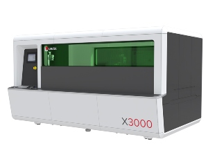
Limata, a provider of Laser Direct Imaging (LDI) systems for PCB manufacturing and adjacent markets, has launched the latest generation of its X3000 LDI system. This platform can handle the largest panels for dry-film patterning and solder mask imaging in PCB production without compromising on its highest precision standards in registration and resolution.
While standard PCB panel sizes have typically measured 24” x 18”, today there is an increasing demand for larger panels, often 24” x 36” or bigger, as well as a need to produce flexible PCBs in non-standard sizes. These large PCBs support a range of growing applications such as LED displays, 5G communications, aerospace and EV-automotive electronics. Using large PCBs instead of a combination of smaller boards delivers superior signal quality or lower signal attenuation in high frequency applications, while at the same time noticeably reducing assembly and installation costs.
Being able to handle large panel formats, up to 110" x 48", also means that the X3000 can simultaneously image multiple smaller PCBs in a single run, for example twelve standard 24" x 18" boards. This increases throughput, by reducing loading and unloading times, which further equates to reduced costs per panel. In addition, work processes can be set flexibly in manufacturing locations, since the X3000 can be loaded and unloaded from the front- and back-side.
"With the X3000, we have built an impressive system that can handle even the biggest oversize boards, whilst still retaining the outstanding accuracy of our X1000 and X2000 models," said Matthias Nagel, CTO of Limata. "In addition, the X3000 also supports roll-to-roll for the handling of endless flexible boards, with the largest PCB manufactured so far measuring 25 metres in length."
Auto-calibration
The X3000 model is market-proven and installed at multiple customer sites. This latest system generation further builds on the X-Series family's proven reliability, and utilizes an integrated auto-calibration system further delivering extremely high accuracy – unprecedented for a system of this size. The system improves registration quality with linear and nonlinear transformations, which are automatically applied in response to any distortion that it detects. In addition to PCB production, this accuracy makes the machine well-suited to applications such as chemical milling and industrial etching.
X3000 machine configurations are available with 2, 3 or 4 laser heads, providing a capacity of up to 24 ultra-violet (UV) lasers in total. A high resolution (HR) option provides an adjustable laser spot size for advanced HDI production, reliably handling dams and spaces down to 2 mil / 50 ?m. The platform uses cost-efficient high energy UV diode-lasers that achieve lifetimes (MTBF) of over 25,000 hours, thus further reducing TCO.
Faster solder mask imaging
Like all X-series system platforms from Limata, for solder mask direct imaging tasks the X3000 can also be equipped with Limata’s innovative LUVIR? technology, which uses a combination of UV and infrared (IR) lasers to reduce UV power consumption. Furthermore, this significantly increases the speed of solder mask (SM) direct imaging and achieves a TCO that is up to 40% lower than competing systems.
Share on:


Testimonial
"Advertising in PCB007 Magazine has been a great way to showcase our bare board testers to the right audience. The I-Connect007 team makes the process smooth and professional. We’re proud to be featured in such a trusted publication."
Klaus Koziol - atgSuggested Items
Indium Experts to Present on Power Electronics at productronica 2025
11/14/2025 | Indium CorporationAs one of the leading materials providers to the power electronics assembly and e-Mobility industries, Indium Corporation® experts will share their technical insight and knowledge on a variety of industry-related topics during Productronica, November 18-21, in Munich, Germany.
ESCATEC Installs Third Wave Soldering Machine in Penang to Meet Growing Demand
11/14/2025 | ESCATECESCATEC’s business unit in Penang, ESCATEC Electronics Sdn Bhd (EEM), recently welcomed the installation of an advanced Ersa POWERFLOW ULTRA wave soldering system, strengthening its capabilities and production capacity for customers bringing complex high-tech products to market.
Mycronic Unveils BA 01 Small Dot Ejector for Next-Generation Precision Jet Printing
11/12/2025 | MycronicMycronic’s BA 01 small dot ejector, delivers unmatched precision in solder paste jet printing for advanced PCB designs.
Indium is Electrifying the Future with Advanced Materials Solutions at productronica
11/11/2025 | Indium CorporationAs one of the leading providers in advanced materials solutions for power device packaging and materials for the electronics assembly and solder industries, Indium Corporation® is proud to feature its lineup of high-reliability products at Productronica, taking place November 18-21, in Munich, Germany.
KOKI to Host Technical Webinar on Dewetting Defects in SMT Soldering
11/11/2025 | KOKIKOKI, a global leader in advanced soldering materials and process solutions, announced its upcoming technical webinar, “Understanding and Preventing Dewetting Defects in SMT Soldering.”