


 The Chemical Connection: Onshoring PCB Production—Daunting but Certainly Possible
 Marcy’s Musings: The Legislative Outlook—Helping or Hurting?
 It’s Only Common Sense: The Phone Is Still Mightier Than the Keyboard


PV Nano Cell Introduces 7 New Digital Conductive Inks
December 14, 2020 | Globe NewswireEstimated reading time: 2 minutes
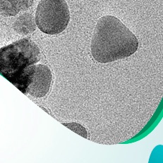
PV Nano Cell Ltd., an innovative provider of inkjet-based conductive digital printing solutions and producer of conductive digital inks, has announced that it is introducing additional digital conductive inks meant for Solar, Ceramic, Glass, LIFT and Generic Applications. The newly introduced inks are meant for the following digital conductive printing technologies: inkjet, aerosol and Laser Induced Forward Transfer.
PV Nano Cell is introducing and making public a total of 7 new digital conductive inks. 2 silver conductive inks for general purpose applications, 2 silver conductive inks with glass frits for solar, ceramic and glass application, 2 copper conductive inks and 1 new copper-based high-viscous ink for LIFT printing. The new inks cover a range of metal loads from 20% to 60% silver or copper, various solvents and optimization to conductive printing technologies including inkjet, aerosol and LIFT.
PV Nano Cell’s Chief Executive Officer, Dr. Fernando de la Vega, commented, “These newly introduced inks are the result of market and customers' requirements that we see growing over the past year. First, in the glass-related industry we see many new applications and use cases emerging for automotive, such as the case with project Tinker we released a PR about most recently. Second, solar-related customers of ours are realizing the phenomenal advantage of using our complete solution in dramatically increasing their overall power efficiency. Last and not least we experience strong demand for additional inks to support a wide array of IoT applications, including sensors, antennas, PCB and medical-related. The ability to introduce new conductive inks heavily relies on our strong IP and patents relating to our Sicrys™ conductive silver and coper inks. This IP allows us to quickly and efficiently respond to market needs and develop and optimize new ink products for our customers.”
PV Nano Cell’s Chief of Business Development Officer, Mr. Hanan Markovich commented, “Our complete solution approach of conductive inks, printers and printing process, naturally leverages our conductive ink technology advantages. Alongside our off the shelf products we are requested to either optimize or develop new inks per specific customer requirements. Our core chemistry competency enables us to fully control properties such as the type of metal, metal load, type of solvent, viscosity, printing technology designation and even the size of the nano-particles. By balancing these properties, we are able to carefully craft superior performing inks to be used in mass-production applications with high-throughput printing. Some of the new ink technologies developed we modify for more general purposes that can be used by many of our customers. These new inks will support the further growth of our business in mass-production applications.”
As most recently published, PV Nano Cell announced that the European Union ?s H2020 funded TINKER project in which the Company is a partner, has started. TINKER is set to develop a new reliable, cost-and resource efficient pathway for automotive RADAR and LiDAR sensor package fabrication based on additive manufacturing.
Share on:


Testimonial
"The I-Connect007 team is outstanding—kind, responsive, and a true marketing partner. Their design team created fresh, eye-catching ads, and their editorial support polished our content to let our brand shine. Thank you all! "
Sweeney Ng - CEE PCBSuggested Items
Episode 6 of Ultra HDI Podcast Series Explores Copper-filled Microvias in Advanced PCB Design and Fabrication
10/15/2025 | I-Connect007I-Connect007 has released Episode 6 of its acclaimed On the Line with... American Standard Circuits: Ultra High Density Interconnect (UHDI) podcast series. In this episode, “Copper Filling of Vias,” host Nolan Johnson once again welcomes John Johnson, Director of Quality and Advanced Technology at American Standard Circuits, for a deep dive into the pros and cons of copper plating microvias—from both the fabricator’s and designer’s perspectives.
Nolan’s Notes: Tariffs, Technologies, and Optimization
10/01/2025 | Nolan Johnson -- Column: Nolan's NotesLast month, SMT007 Magazine spotlighted India, and boy, did we pick a good time to do so. Tariff and trade news involving India was breaking like a storm surge. The U.S. tariffs shifted India from one of the most favorable trade agreements to the least favorable. Electronics continue to be exempt for the time being, but lest you think that we’re free and clear because we manufacture electronics, steel and aluminum are specifically called out at the 50% tariff levels.
MacDermid Alpha & Graphic PLC Lead UK’s First Horizontal Electroless Copper Installation
09/30/2025 | MacDermid Alpha & Graphic PLCMacDermid Alpha Electronics Solutions, a leading supplier of integrated materials and chemistries to the electronics industry, is proud to support Graphic PLC, a Somacis company, with the installation of the first horizontal electroless copper metallization process in the UK.
Electrodeposited Copper Foils Market to Grow by $11.7 Billion Over 2025-2032
09/18/2025 | Globe NewswireThe global electrodeposited copper foils market is poised for dynamic growth, driven by the rising adoption in advanced electronics and renewable energy storage solutions.
MacDermid Alpha Showcases Advanced Interconnect Solutions at PCIM Asia 2025
09/18/2025 | MacDermid Alpha Electronics SolutionsMacDermid Alpha Electronic Solutions, a global leader in materials for power electronics and semiconductor assembly, will showcase its latest interconnect innovations in electronic interconnect materials at PCIM Asia 2025, held from September 24 to 26 at the Shanghai New International Expo Centre, Booth N5-E30