


 Trouble in Your Tank: Understanding Interconnect Defects, Part 1
 It’s Only Common Sense: Marketing Isn’t Fluff, It’s Ammunition
 Driving Innovation: Mechanical and Optical Processes During Rigid-flex Production


ESI Supplies Model 5335 Laser Processing System to PFC
June 9, 2015 | Business WireEstimated reading time: 2 minutes
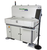
Electro Scientific Industries, Inc., an innovator in laser-based manufacturing solutions for the micro-machining industry, today announced that PFC Flexible Circuits Limited has selected the Model 5335 Laser Processing System to expand its high density interconnect (HDI) flexible circuit manufacturing capabilities. Based in Scarborough, Ont., Canada, PFC is a North American leader in flexible circuit design, manufacture and assembly.
“PFC has been supplying fine line technology for the past eight years. Now, with the addition of the Model 5335, we can support true HDI flex technologies,” said Steve Kelly, President of PFC Flexible Circuits. “This laser processing system from ESI will allow us to make smaller vias, blind and buried vias, and to cut smaller features in HDI circuits. We’re seeing strong market interest in HDI across multiple industries ranging from consumer and medical devices to military and aerospace.”
PFC chose the ESI Model 5335 in part because of its high throughput capabilities compared to alternatives. For example, the ESI Model 5335 can drill 50 micron blind vias at a rate of 32,000 holes per minute. This performance is made possible by Third Dynamics™, a patented high-speed beam positioning technology that enables fast and accurate routing and drilling of flexible circuits.
“We were looking to update our drilling technology without losing throughput,” said Anish Somaiya, Vice President, PFC Flexible Circuits. “The Model 5335 not only will significantly increase our drilling throughput and give us a technological edge over many of our competitors but also will save floor space in our drilling area.”
The ESI Model 53XX family is widely regarded as the industry standard for laser processing across the flexible circuit and interconnect industry. Over 1,200 ESI laser processing systems are installed worldwide and are in use at nine of the top 10 flex circuit manufacturers. These systems offer industry-leading drill, routing, patterning, and skiving performance.
“We are extremely pleased that PFC has decided to incorporate ESI laser processing technology into its HDI and flexible circuit manufacturing processes,” said Ed Grady, CEO of ESI. “We look forward to being a part of PFC’s long-term success and helping them meet their most challenging customer demands.”
About PFC
PFC Flexible Circuits designs, manufactures and assembles flexible printed circuits, all under one roof. Circuit types include single- and double-sided, multi-layer and rigid flex. PFC can provide 50 micron line and space in production and assemble circuits using 1005 components. Specialties include high-speed low-loss, impedance-controlled circuits. PFC offers a large library of UL approved materials and is ISO 9001 and 13485 approved. For more information go to: www.pfcflex.com.
About ESI
ESI's integrated solutions allow industrial designers and process engineers to control the power of laser light to transform materials in ways that differentiate their consumer electronics, wearable devices, semiconductor circuits and high-precision components for market advantage. ESI's laser-based manufacturing solutions feature the micro-machining industry's highest precision and speed, and target the lowest total cost of ownership. ESI is headquartered in Portland, Ore., with global operations from the Pacific Northwest to the Pacific Rim. More information is available at www.esi.com.
Share on:


Testimonial
"Your magazines are a great platform for people to exchange knowledge. Thank you for the work that you do."
Simon Khesin - Schmoll MaschinenSuggested Items
Photonics Systems Group Announces Exclusive After-Hours Tech Event at productronica 2025
11/05/2025 | Photonics Systems GroupPhotonics Systems Group (PSG), a leading expert in laser micromachining specifically for the electronics industry, announced its inaugural after-hours technical event, the Photonics Tech Evening, to be held on November 19, 2025, during Productronica 2025.
Learning With Leo: UHDI—The Next Leap in PCB Manufacturing
11/05/2025 | Leo Lambert -- Column: Learning With LeoHigh density interconnect (HDI) technology has been a cornerstone of miniaturized electronics since Hewlett-Packard introduced the first chip-scale implementation in 1982. Over time, HDI processes became central to organic flip-chip packaging in the semiconductor industry. Today, the convergence of IC substrates and system-level PCBs has accelerated the adoption of UHDI.
EMS and ODM Market Size to Surpass USD 1589.62 Billion by 2033, Rising at 7.40% CAGR
11/04/2025 | Globe NewswireAccording to the SNS Insider, “The EMS and ODM market size was valued at USD 900.09 Billion in 2025E and is projected to reach USD 1,589.62 Billion by 2033, growing at a CAGR of 7.40% during 2026–2033.”
Electronics Manufacturing Powers U.S. Growth, Supporting 5.2 Million Jobs and $1.8 Trillion in Output
11/03/2025 | Global Electronics AssociationNew report from Global Electronics Association shows electronics industry contributes $853 billion to GDP and delivers average annual wages exceeding $156,000, reinforcing its role as a pillar of U.S. economic resilience.
Nolan’s Notes: Is Mexico the Pulse of Electronics in the Americas?
11/04/2025 | Nolan Johnson -- Column: Nolan's NotesLast year, I attended SMTA Guadalajara, where I saw the results of the Mexican investment in electronics manufacturing. The U.S. was still operating under the Biden administration, and while Mexican EMS companies had expanded capacity to support EV manufacturing, the demand dropped significantly. In my conversations at the show, the sentiment was one of patience. They knew the EV business would likely come back. However, they didn’t expect an overhaul of U.S. trade agreements and tariffs that would shift a more diversified portfolio in Mexico’s direction.