


 The Chemical Connection: Onshoring PCB Production—Daunting but Certainly Possible
 It’s Only Common Sense: The Phone Is Still Mightier Than the Keyboard


New Sensing Technology Could Improve Ability to Detect
June 10, 2015 | University at BuffaloEstimated reading time: 3 minutes
From airport security detecting explosives to art historians authenticating paintings, society’s thirst for powerful sensors is growing.
Given that, few sensing techniques can match the buzz created by surface-enhanced Raman spectroscopy (SERS).
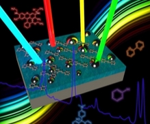
Discovered in the 1970s, SERS is a sensing technique prized for its ability to identify chemical and biological molecules in a wide range of fields. It has been commercialized, but not widely, because the materials required to perform the sensing are consumed upon use, relatively expensive and complicated to fabricate.
That may soon change.
An international research team led by University at Buffalo engineers has developed nanotechnology that promises to make SERS simpler and more affordable.
Described in a research paper published in the journal Advanced Materials Interfaces, the photonics advancement aims to improve our ability to detect trace amounts of molecules in diseases, chemical warfare agents, fraudulent paintings, environmental contaminants and more.
“The technology we’re developing – a universal substrate for SERS – is a unique and, potentially, revolutionary feature. It allows us to rapidly identify and measure chemical and biological molecules using a broadband nanostructure that traps wide range of light,” said Qiaoqiang Gan, UB assistant professor of electrical engineering and the study’s lead author.
Additional authors of the study are: UB PhD candidates in electrical engineering Nan Zhang, Kai Liu, Haomin Song, Xie Zeng, Dengxin Ji and Alec Cheney; and Suhua Jiang, associate professor of materials science, and Zhejun Liu, PhD candidate, both at Fudan University in China.
When a powerful laser interacts chemical and biological molecules, the process can excite vibrational modes of these molecules and produce inelastic scattering, also called Raman scattering, of light. As the beam hits these molecules, it can produce photons that have a different frequency from the laser light. While rich in details, the signal from scattering is weak and difficult to read without a very powerful laser.
SERS addresses the problem by utilizing a nanopatterned substrate that significantly enhances the light field at the surface and, therefore, the Raman scattering intensity. Unfortunately, traditional substrates are typically designed for only a very narrow range of wavelengths. This is problematic because different substrates are needed if scientists want to use a different laser to test the same molecules. In turn, this requires more chemical molecules and substrates, increasing costs and time to perform the test.
The universal substrate solves the problem because it can trap a wide range of wavelengths and squeeze them into very small gaps to create a strongly enhanced light field.
The technology consists of a thin film of silver or aluminum that acts as a mirror, and a dielectric layer of silica or alumina. The dielectric separates the mirror with tiny metal nanoparticles randomly spaced at the top of the substrate.
“It acts similar to a skeleton key. Instead of needing all these different substrates to measure Raman signals excited by different wavelengths, you’ll eventually need just one. Just like a skeleton key that opens many doors,” Zhang said.
“The applications of such a device are far-reaching,” said Kai Liu. “The ability to detect even smaller amounts of chemical and biological molecules could be helpful with biosensors that are used to detect cancer, Malaria, HIV and other illnesses.”
It could be useful identifying chemicals used in certain types of paint. This could be helpful detecting forged pieces of art as well as restoring aging pieces of art. Also, the technology could improve scientists’ ability to detect trace amounts of toxins in the air, water or other spaces that are causes for health concerns. And it could aid in the detection of chemical weapons.
The National Science Foundation supported the research in a grant to develop a real-time in-vivo biosensing system. Gan shares the grant with Josep M. Jornet and Zhi Sun, both assistant professors of electrical engineering at UB.
Gan is a member of UB’s electrical engineering optics and photonics research group, which includes professors Edward Furlani, Natalia Litchinitser and Pao-Lo Liu; and assistant professor Liang Feng.
The group carries out research in nanophotonics, biophotonics, hybrid inorganic/organic materials and devices, nonlinear and fiber optics, metamaterials, nanoplasmonics, optofluidics, microelectromechanical systems (MEMS), biomedical microelectromechanical systems (BioMEMs), biosensing and quantum information processing.
Share on:


Testimonial
"In a year when every marketing dollar mattered, I chose to keep I-Connect007 in our 2025 plan. Their commitment to high-quality, insightful content aligns with Koh Young’s values and helps readers navigate a changing industry. "
Brent Fischthal - Koh YoungSuggested Items
ITW EAE Despatch Ovens Now Support ASTM 5423 Testing
10/15/2025 | ITW EAEAs the demand for high-performance electrical insulation materials continues to grow—driven by the rapid expansion of electric vehicles (EVs) and energy storage systems—thermal processing has become a critical step in material development.
Beyond Thermal Conductivity: Exploring Polymer-based TIM Strategies for High-power-density Electronics
10/13/2025 | Padmanabha Shakthivelu and Nico Bruijnis, MacDermid Alpha Electronics SolutionsAs power density and thermal loads continue to increase, effective thermal management becomes increasingly important. Rapid and efficient heat transfer from power semiconductor chip packages is essential for achieving optimal performance and ensuring long-term reliability of temperature-sensitive components. This is particularly crucial in power systems that support advanced applications such as green energy generation, electric vehicles, aerospace, and defense, along with high-speed computing for data centers and artificial intelligence (AI).
Is Glass Finally Coming of Age?
10/13/2025 | Nolan Johnson, I-Connect007Substrates, by definition, form the base of all electronic devices. Whether discussing silicon wafers for semiconductors, glass-and-epoxy materials in printed circuits, or the base of choice for interposers, all these materials function as substrates. While other substrates have come and gone, silicon and FR-4 have remained the de facto standards for the industry.
Creative Materials to Showcase Innovative Functional Inks for Medical Devices at COMPAMED 2025
10/09/2025 | Creative Materials, Inc.Creative Materials, a leading manufacturer of high-performance functional inks and coatings, is pleased to announce its participation in COMPAMED 2025, taking place November 17–20 in Düsseldorf, Germany.
Jiva Leading the Charge Toward Sustainable Innovation
09/30/2025 | Marcy LaRont, PCB007 MagazineEnvironmental sustainability in business—product circularity—is a high priority these days. “Circularity,” the term meant to replace “recycling,” in its simplest definition, describes a full circle life for electronic products and all their elements. The result is re-use or a near-complete reintroduction of the base materials back into the supply chain, leaving very little left for waste. For what cannot be reused productively, the ultimate hope is to have better, less harmful means of disposal and/or materials that can seamlessly and harmlessly decompose and integrate back into the natural environment. That is where Jiva and Soluboard come in.