


 Knocking Down the Bone Pile: Revamp Your Components with BGA Reballing
 Global Sourcing Spotlight: Balancing Speed and Flexibility Without Sacrificing Control
 SMT Perspectives & Prospects: Artificial Intelligence Part 6: Data Module 1


In-line Solder Penetration Testing with 3D X-ray Inspection
June 10, 2015 | Andreas Turk, Goepel ElectronicEstimated reading time: 2 minutes
Through-hole technology (THT) is probably the oldest assembly technology in the field of PCB manufacturing. However, even in this modern age of surface-mounted technology (SMT), it still has its place. Even today, wired components are often assembled using wave soldering—in keeping with the tradition of times past. This has the disadvantage of requiring additional manufacturing equipment. It is therefore advisable to use reflow soldering for connectors and other wired components.
To this end, through-hole components were devised for automatic assembly and for high thermal loads in the furnace, which led to the birth of the term, through-hole reflow (THR). With this technology, it is now possible to process components in through-hole technology within the SMT process. But how can these solder joints be reliably tested? What technology is needed in order to be able to assess the solder penetration, for example?
Acceptance Criteria for THT/THR Solder Joints
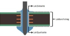
Figure 1 is a schematic representation of a THT solder joint in cross-section. The solder wave flows from the solder source side to the solder target side (component side), due to capillary action. In so doing, it wets the connecting surface of the solder side, surrounds the pin and forms a solder meniscus on account of the protrusion of the pin on the solder side.
The acceptance criteria are defined in IPCA610 in order to distinguish between good and bad solder joints after successful soldering. Table 1 gives an overview of the criteria in excerpts.
It is now necessary to select testing technology which meets the specified acceptance criteria. Based on the example of a multi-row connector (Figure 2), the following table provides an overview of the test coverage of AOI and 3D AXI systems.
AOI systems are highly suited to assessment of the peripheral wetting of the pin and the sleeve and to evaluation of the wetted connecting surface on the solder side of a THT solder joint. The disadvantage of a traditional 2D AOI or an innovative 3D AOI system here, however, is that it is often only possible to assess the solder side because the pins on the component side are usually concealed by the component body itself. An assessment of the solder joints on the component side is therefore not possible with an AOI system. The solder penetration also remains hidden from traditional AOI technology.
A modern 3D X-ray system can provide a remedy. The 3D X-ray inspection not only makes the solder joints on the component side (i.e., below the component housing) visible, but is also able to calculate the solder penetration and the solder volume.
Editor's Note: This article originally appeared in the June 2015 issue of SMT Magazine.
Share on:


Testimonial
"In a year when every marketing dollar mattered, I chose to keep I-Connect007 in our 2025 plan. Their commitment to high-quality, insightful content aligns with Koh Young’s values and helps readers navigate a changing industry. "
Brent Fischthal - Koh YoungSuggested Items
Rehm Wins Mexico Technology Award for CondensoXLine with Formic Acid
10/17/2025 | Rehm Thermal SystemsModern electronics manufacturing requires technologies with high reliability. By using formic acid in convection, condensation, and contact soldering, Rehm Thermal Systems’ equipment ensures reliable, void-free solder joints — even when using flux-free solder pastes.
Indium Experts to Deliver Technical Presentations at SMTA International
10/14/2025 | Indium CorporationAs one of the leading materials providers to the power electronics assembly industry, Indium Corporation experts will share their technical insight on a wide range of innovative solder solutions at SMTA International (SMTAI), to be held October 19-23 in Rosemont, Illinois.
Knocking Down the Bone Pile: Revamp Your Components with BGA Reballing
10/14/2025 | Nash Bell -- Column: Knocking Down the Bone PileBall grid array (BGA) components evolved from pin grid array (PGA) devices, carrying over many of the same electrical benefits while introducing a more compact and efficient interconnect format. Instead of discrete leads, BGAs rely on solder balls on the underside of the package to connect to the PCB. In some advanced designs, solder balls are on both the PCB and the BGA package. In stacked configurations, such as package-on-package (PoP), these solder balls also interconnect multiple packages, enabling higher functionality in a smaller footprint.
Indium to Showcase High-Reliability Solder and Flux-Cored Wire Solutions at SMTA International
10/09/2025 | Indium CorporationAs one of the leading materials providers in the electronics industry, Indium Corporation® will feature its innovative, high-reliability solder and flux-cored wire products at SMTA International (SMTAI), to be held October 19-23 in Rosemont, Illinois.
‘Create your Connections’ – Rehm at productronica 2025 in Munich
10/08/2025 | Rehm Thermal SystemsThe electronics industry is undergoing dynamic transformation: smart production lines, sustainability, artificial intelligence, and sensor technologies dominate current discussions.