


 The Chemical Connection: Onshoring PCB Production—Daunting but Certainly Possible
 It’s Only Common Sense: The Phone Is Still Mightier Than the Keyboard


Surfaces Get Smooth or Bumpy on Demand
June 12, 2015 | MITEstimated reading time: 3 minutes
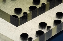
An MIT team has developed a way of making soft materials, using a 3-D printer, with surface textures that can then be modified at will to be perfectly smooth, or ridged or bumpy, or even to have complex patterns that could be used to guide fluids.
The process, developed using detailed computer simulations, involves a material that is composed of two different polymers with different degrees of stiffness: More rigid particles are embedded within a matrix of a more flexible polymer. When squeezed, the material’s surface changes from smooth to a pattern determined by the spacing and shapes of the implanted harder particles; when released, it reverts back to the original form.
The findings, which the researchers say could lead to a new class of materials with dynamically controllable and reversible surface properties, are reported in a paper in the journal Advanced Functional Materials co-authored by MIT graduate student Mark Guttag and Mary Boyce, a former MIT professor of mechanical engineering who is now dean of engineering at Columbia University.
“Depending on the arrangement of the particles, using the same amount of compression, you can get different surface topographies, including ridges and bumps, along the surface,” says Guttag, who is pursuing the research as part of his doctoral thesis in mechanical engineering.
The system can produce simple, repetitive patterns of bumps or creases, which could be useful for changing the aerodynamic resistance of an object, or its reflectivity. But by arranging the distribution of the hard particles, it can also be used to produce highly complex surface textures — for example, creating microfluidic channels to control the movement of liquids inside a chemical or biological detector, Guttag says.
For instance, such a device could have a smooth, tilted surface allowing fluids to flow evenly across its surface — but with the added ability, on demand, to create raised sections and depressions that would separate the flow of liquids.
Surface textures can be important in a variety of applications, including camouflage, making surfaces that repel or attract water, controlling the motion and turbulence of fluids, and limiting the buildup of organisms on surfaces such as ship hulls. There are many ways to produce patterning as a fixed, unvarying surface, but for some uses — including drag reduction and camouflage — changeable and nonuniform textures could have added benefit.
“There are no previous techniques that provide comparable flexibility for creating dynamically and locally tunable and reversible surface changes,” Guttag and Boyce write in their paper.
Because the system is “all geometry driven,” Guttag says — based on the shapes and spacing of materials with different degrees of flexibility — “it could be scaled to all different sizes, and the same principles should work.”
While this research used physical pressure to control texture, the same design principles could be used to modify materials using other stimuli — such as through application of an electric charge, or by changing temperature or humidity, Guttag adds.
Using embedded particles that are elongated instead of round could also allow for the creation of surface textures that are asymmetrical. This could, for example, create surfaces that have high friction in one direction but are slippery in another, allowing a passive means of controlling how things move over that surface.
The initial development of the system was done using computer simulations, which were then validated by making 3-D-printed versions of several of the designs. The surface patterns were produced when the soft printed materials were compressed closely matched those seen in the simulations, Guttag says.
“This is the first-of-its-kind work to create materials with reconfigurable surface texture,” says Yonggang Huang, a professor of civil and environmental engineering and mechanical engineering at Northwestern University who was not involved in this work. He adds, “The potential practical impact of this work is huge. It can be used in many applications that benefit from the change of surface, such as in optics and tribology [the science of interacting surfaces in motion].” Huang compares this to the development of 3-D printing, saying “once the method is developed, people can use it creatively in numerous applications.”
The project was funded through a cooperative agreement between the Masdar Institute of Science and Technology and MIT.
Share on:


Testimonial
"We’re proud to call I-Connect007 a trusted partner. Their innovative approach and industry insight made our podcast collaboration a success by connecting us with the right audience and delivering real results."
Julia McCaffrey - NCAB GroupSuggested Items
ITW EAE Despatch Ovens Now Support ASTM 5423 Testing
10/15/2025 | ITW EAEAs the demand for high-performance electrical insulation materials continues to grow—driven by the rapid expansion of electric vehicles (EVs) and energy storage systems—thermal processing has become a critical step in material development.
Beyond Thermal Conductivity: Exploring Polymer-based TIM Strategies for High-power-density Electronics
10/13/2025 | Padmanabha Shakthivelu and Nico Bruijnis, MacDermid Alpha Electronics SolutionsAs power density and thermal loads continue to increase, effective thermal management becomes increasingly important. Rapid and efficient heat transfer from power semiconductor chip packages is essential for achieving optimal performance and ensuring long-term reliability of temperature-sensitive components. This is particularly crucial in power systems that support advanced applications such as green energy generation, electric vehicles, aerospace, and defense, along with high-speed computing for data centers and artificial intelligence (AI).
Is Glass Finally Coming of Age?
10/13/2025 | Nolan Johnson, I-Connect007Substrates, by definition, form the base of all electronic devices. Whether discussing silicon wafers for semiconductors, glass-and-epoxy materials in printed circuits, or the base of choice for interposers, all these materials function as substrates. While other substrates have come and gone, silicon and FR-4 have remained the de facto standards for the industry.
Creative Materials to Showcase Innovative Functional Inks for Medical Devices at COMPAMED 2025
10/09/2025 | Creative Materials, Inc.Creative Materials, a leading manufacturer of high-performance functional inks and coatings, is pleased to announce its participation in COMPAMED 2025, taking place November 17–20 in Düsseldorf, Germany.
Jiva Leading the Charge Toward Sustainable Innovation
09/30/2025 | Marcy LaRont, PCB007 MagazineEnvironmental sustainability in business—product circularity—is a high priority these days. “Circularity,” the term meant to replace “recycling,” in its simplest definition, describes a full circle life for electronic products and all their elements. The result is re-use or a near-complete reintroduction of the base materials back into the supply chain, leaving very little left for waste. For what cannot be reused productively, the ultimate hope is to have better, less harmful means of disposal and/or materials that can seamlessly and harmlessly decompose and integrate back into the natural environment. That is where Jiva and Soluboard come in.