


 Knocking Down the Bone Pile: Gold Mitigation for Class 2 Electronics
 Punching Out: Your Financial Preparation for a Sale
 Nolan's Notes: The Next Killer App in Component Manufacturing


Meaningful SPI Production Control Through Automatic Normalization
June 15, 2015 | MEKEstimated reading time: 3 minutes
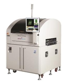
Automated pre-placement solder paste inspection (SPI) has established itself in SMT assembly as an essential tool for optimizing the process and reducing end of line defects. It’s been commonly accepted for many years that a majority of assembly defects can be traced back to print defects, and by using raw measurement data from printed PCBs for volume, area, height and offset, SPC histograms and control charts can quite readily be used to optimize the process.
Following optimization, SPI is used to detect print anomalies. However, the multitude of “normal” variables introduced from board characteristics, clamping methodologies, stencil variations and paste type force unacceptably wide tolerance settings. These board-wide good/bad tolerances can easily mount to +/- 50% or more. For most, this is unacceptable, because of course, with such wide tolerances production drift can be missed and important defects ignored.
Tolerances before and after Optimization are similar
Aperture Release
For example, stencil pattern variations cause differences between designed (expected) and actual solder release. For large apertures, release variation is generally negligible. Small apertures can account for up to 50% release variation or even more. Stencil thickness to aperture area ratio determines how close to 100% release efficiency is achievable. As pads get smaller and smaller, the area of the aperture wall approaches that of the pad area. In turn, the paste release efficiency is reduced as the adhesion forces from the walls approach that of the pad. Thus, different pad sizes across a board will exhibit different volume performance.
A common work-around for this is possible by selecting specific areas and setting tolerances for these apertures.
Though these custom tolerance settings may be individually easy to perform, they are time consuming and do not carry over to other PCB’s due to differences in design, manufacture and finish. These differences are common practice in just in time manufacturing:
1. Solder mask thickness variations; typical thickness 25 um +25/– 12um; Silk screen legends can add 12 um
2. Solder mask defined or non solder mask defined apertures
3. Gasketing effect variations
4. Solder pad finish
a. OSP and gold 0 %variation
b. HASL +/-20 um
5. Board Warpance:
These all create variations on the “zero reference height” point on each pad for measurement.
Mek Automated Normalization
Automated Normalization has been introduced by Mek SPI which directly addresses the excessive time required for board region based tolerance tightening. This unique 2 stage system allows the user to first optimize the printing process and then once the optimization has been completed, to automatically normalise the results and then set tighter tolerances to monitor product drift, enabling meaningful production control. The 5D measurement, combining 2D and 3D measurements ensures proper zero referencing, forming a solid base for accurate and repeatable measurements.
Tolerances after Normalization
The normalization extraction takes user selected average area, height and volume from several previous inspections when being set. Thus, an accurate representation of the capability of the print process is incorporated. If a process change, such as stencil or print settings need be made, the normalization extraction can be readily reset and then applied once again. www.marantz-electronics.com
About MEK (Marantz Electronics Ltd)
A former division of Marantz well known for its high quality Audio/Video products, MEK Japan (Marantz Electronics Kabushiki Kaisha), developed its first AOI system in 1994. Developed to inspect PCB assemblies for correct component placement and soldering, the company’s original AOI system was designed for use in Marantz factories. Proving to be a highly successful, cost-effective alternative to traditional human inspection, MEK developed its first generation commercial system in 1996. With a steadily growing installed base, MEK Japan and its European/American headquarters, MEK, have sold over 5000 units worldwide to date. Now well established as a leading force in AOI technologies, the company recently launched a 5D post-print SPI system which combines 3D and 2D image processing methodologies to deliver unprecedented defect detection. At the beginning of March 2014 the company opened US offices in Las Vegas.
Share on:


Suggested Items
Indium’s Karthik Vijay to Present on Dual Alloy Solder Paste Systems at SMTA’s Electronics in Harsh Environments Conference
05/06/2025 | Indium CorporationIndium Corporation Technical Manager, Europe, Africa, and the Middle East Karthik Vijay will deliver a technical presentation on dual alloy solder paste systems at SMTA’s Electronics in Harsh Environments Conference, May 20-22 in Amsterdam, Netherlands.
SolderKing Achieves the Prestigious King’s Award for Enterprise in International Trade
05/06/2025 | SolderKingSolderKing Assembly Materials Ltd, a leading British manufacturer of high-performance soldering materials and consumables, has been honoured with a King’s Award for Enterprise, one of the UK’s most respected business honours.
Knocking Down the Bone Pile: Gold Mitigation for Class 2 Electronics
05/07/2025 | Nash Bell -- Column: Knocking Down the Bone PileIn electronic assemblies, the integrity of connections between components is paramount for ensuring reliability and performance. Gold embrittlement and dissolution are two critical phenomena that can compromise this integrity. Gold embrittlement occurs when gold diffuses into solder joints or alloys, resulting in mechanical brittleness and an increased susceptibility to cracking. Conversely, gold dissolution involves the melting away of gold into solder or metal matrices, potentially altering the electrical and mechanical properties of the joint.
'Chill Out' with TopLine’s President Martin Hart to Discuss Cold Electronics at SPWG 2025
05/02/2025 | TopLineBraided Solder Columns can withstand the rigors of deep space cold and cryogenic environments, and represent a robust new solution to challenges facing next generation large packages in electronics assembly.
BEST Inc. Reports Record Demand for EZReball BGA Reballing Process
05/01/2025 | BEST Inc.BEST Inc., a leader in electronic component services, is pleased to announce they are experiencing record demand for their EZReball™ BGA reballing process which greatly simplifies the reballing of ball grid array (BGA) and chip scale package (CSP) devices.