


 It’s Only Common Sense: Stop Pretending Your Customers Are Loyal
 Happy’s Tech Talk #44: Memories of the ‘Mystery Systems of the East’


Transition from Three to Two Dimensions Increases Conduction
August 5, 2015 | MIPTEstimated reading time: 2 minutes
Scientists from the MIPT Department of Molecular and Chemical Physics have for the first time described the behavior of electrons in a previously unstudied analogue of graphene, two-dimensional niobium telluride, and, in the process, uncovered the nature of two-dimensionality effects on conducting properties. These findings will help in the creation of future flat and flexible electronic devices.
In recent decades, physicists have been actively studying so-called two-dimensional materials. Andrei Geim and Konstantin Novoselov received the Nobel Prize for their research on graphene, the most well-known among them. The properties of such materials, which can be described as “sheets” with a thickness of a few atoms, strongly differ from their three-dimensional analogues. For example, graphene is transparent, conducts current better than copper and has good thermal conductivity. Scientists believe that other types of two-dimensional materials may possess even more exotic properties.
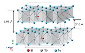
A group of scientists from Russia and the USA, including Pavel Sorokin and Liubov Antipina from MIPT, recently conducted research on the properties of the crystals of one such material,Nb3SiTe6, a compound of niobium telluride. In their structure, the crystals resemble sandwiches with a thickness of three atoms (around 4 angstroms): a layer of tellurium, a layer of niobium mixed with silicon atoms and then another layer of tellurium. This substance belongs to a class of materials known as dichalcogenides, which many scientists view as promising two-dimensional semiconductors.
The scientists synthesized Nb3SiTe6 crystals in a laboratory at Tulane University (New Orleans). They then separated them into two-dimensional layers, taking samples for further analysis by transmission electron microscopy, X-ray crystal analysis and other methods. The goal of the researchers was to investigate electron-phonon interaction changes in two-dimensional substances.
Quasi particles, quanta of crystal lattice oscillations, are called phonons. Physicists introduced the concept of phonons because it helped simplify the description of processes in crystals, and tracking of electron-phonon interaction is fundamentally important for description of the different conducting properties in matter.
"We developed a theory that predicts that electron-phonon interaction is suppressed due to dimensional effects in two-dimensional material. In other words, these materials obstruct the flow of electrons to a lesser extent," says Pavel Sorokin, a co-author of the study, doctor of physical and mathematical sciences, and lecturer at the MIPT Section of the Physics and Chemistry of Nanostructures (DMCP).
American colleagues confirmed this predictioninrelatedexperiments. "They conducted measurements where the same effectwas observed. Our calculations allowed the ruling out of other explanations; we managed to prove that changes in electron-phonon interaction occur specifically because of the two-dimensionality of the membrane," Sorokin adds.
Share on:


Testimonial
"We’re proud to call I-Connect007 a trusted partner. Their innovative approach and industry insight made our podcast collaboration a success by connecting us with the right audience and delivering real results."
Julia McCaffrey - NCAB GroupSuggested Items
The Impact of the AI Boom on PCB and Raw Materials Supply Chains
11/13/2025 | Mark Goodwin, Ventec International GroupThe PCB industry is entering a period of unprecedented structural change, driven by the demands of artificial intelligence and advanced computing. What was once a cyclical market has become a capacity race. It’s one that rewards foresight, collaboration, and strategic supply partnerships. Understanding these dynamics is essential for maintaining stability and growth across all market segments. This report, created by Ventec International Group, provides a clear view of how AI-driven demand is reshaping the PCB materials landscape and what actions are required to secure long-term supply.
Elementary, Mr. Watson: The Four Horsemen of Copper Confusion
11/12/2025 | John Watson -- Column: Elementary, Mr. WatsonIf there were a PCB Design Dictionary of Confusing Terms, the cover would feature four words that have baffled generations of engineers: polygons, pours, planes, and floods—or what I refer to as the four horsemen of copper confusion. They sound simple, as if they belong in a geometry textbook or a weather report, but in PCB design, they overlap, develop, and sound interchangeable until you realize they aren't.
Alpha Insights, Performance by Design: Understanding Heat at the Core of Every Design
11/11/2025 | Team Alpha -- Column: Alpha Insights: Performance by DesignPower isn’t just about current. It’s about control. As electronic systems grow smaller and faster, every amp and every layer generates a new source of heat. That heat is more than a byproduct. It’s a measure of efficiency, a benchmark of performance, and often the first indication of failure.
The Shaughnessy Report: Zee Plane! Zee Plane!
11/11/2025 | Andy Shaughnessy -- Column: The Shaughnessy ReportPlanes aren’t magic, but they are big time-savers. Without planes, designers would have to create thousands of traces to accomplish the same objectives. You can imagine the first time a designer thought about using a sheet of copper, asking, “Hey, why am I killing myself laying out all these traces? Can’t I just use this sheet of copper instead?”
November 2025 Design007 Magazine: Proper Plane Design
11/10/2025 | I-Connect007 Editorial TeamWithout planes, designers would have to create thousands of traces to accomplish the same objectives. Power planes provide low impedance and stable power to every component on the board, much like a large power bus. Ground planes stabilize reference voltage, improve thermal performance, and help preclude EMI issues. Power and ground plane design is often a battle of tradeoffs.