


 Trouble in Your Tank: Understanding Interconnect Defects, Part 1
 It’s Only Common Sense: Marketing Isn’t Fluff, It’s Ammunition
 Driving Innovation: Mechanical and Optical Processes During Rigid-flex Production


MechSE Researchers Create One-step Graphene Patterning Method
April 28, 2016 | University of IllinoisEstimated reading time: 2 minutes
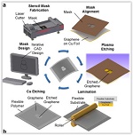
Researchers from the University of Illinois at Urbana-Champaign have developed a one-step, facile method to pattern graphene by using stencil mask and oxygen plasma reactive-ion etching, and subsequent polymer-free direct transfer to flexible substrates.
Graphene, a two-dimensional carbon allotrope, has received immense scientific and technological interest. Combining exceptional mechanical properties, superior carrier mobility, high thermal conductivity, hydrophobicity, and potentially low manufacturing cost, graphene provides a superior base material for next generation bioelectrical, electromechanical, optoelectronic, and thermal management applications.
“Significant progress has been made in the direct synthesis of large-area, uniform, high quality graphene films using chemical vapor deposition (CVD) with various precursors and catalyst substrates,” explained SungWoo Nam, an assistant professor of mechanical science and engineeringat Illinois. “However, to date, the infrastructure requirements on post-synthesis processing—patterning and transfer—for creating interconnects, transistor channels, or device terminals have slowed the implementation of graphene in a wider range of applications.”“In conjunction with the recent evolution of additive and subtractive manufacturing techniques such as 3D printing and computer numerical control milling, we developed a simple and scalable graphene patterning technique using a stencil mask fabricated via a laser cutter,” stated Keong Yong, a graduate student and first author of the paper, “Rapid Stencil Mask Fabrication Enabled One-Step Polymer-Free Graphene Patterning and Direct Transfer for Flexible Graphene Devices" appearing in Scientific Reports.
“Our approach to patterning graphene is based on a shadow mask technique that has been employed for contact metal deposition,” Yong added. “Not only are these stencil masks easily and rapidly manufactured for iterative rapid prototyping, they are also reusable, enabling cost-effective pattern replication. And since our approach involves neither a polymeric transfer layer nor organic solvents, we are able to obtain contamination-free graphene patterns directly on various flexible substrates.”Nam stated that this approach demonstrates a new possibility to overcome limitations imposed by existing post-synthesis processes to achieve graphene micro-patterning. Yong envisions this facile approach to graphene patterning sets forth transformative changes in “do It yourself” (DIY) graphene-based device development for broad applications including flexible circuits/devices and wearable electronics.
“This method allows rapid design iterations and pattern replications, and the polymer-free patterning technique promotes graphene of cleaner quality than other fabrication techniques,” Nam said. “We have shown that graphene can be patterned into varying geometrical shapes and sizes, and we have explored various substrates for the direct transfer of the patterned graphene.”
In addition to Nam and Yong, study co-authors include Ali Ashraf and Pilgyu Kang from the Department of Mechanical Science and Engineering at Illinois.
Share on:


Testimonial
"In a year when every marketing dollar mattered, I chose to keep I-Connect007 in our 2025 plan. Their commitment to high-quality, insightful content aligns with Koh Young’s values and helps readers navigate a changing industry. "
Brent Fischthal - Koh YoungSuggested Items
Driving Innovation: Mechanical and Optical Processes During Rigid-flex Production
10/28/2025 | Kurt Palmer -- Column: Driving InnovationRigid-flex printed circuit boards are a highly effective solution for placing complex circuitry in tight, three-dimensional spaces. They are now indispensable across a range of industries, from medical devices and aerospace to advanced consumer electronics, helping designers make the most efficient use of available space. However, their unique construction—combining rigid and flexible materials—presents a fundamental challenge for PCB manufacturers.
Elkem Launches Biocompatible, Conductive SILBIONE LSR for Advanced Medical Devices
10/23/2025 | PRNewswireElkem ASA, a global leader in advanced silicon-based materials, unveiled SILBIONE LSR Select EC 70, a next-generation medical-grade liquid silicone rubber. Designed for wearable and diagnostic devices, the material combines high electrical conductivity, certified biocompatibility1, and enhanced process control, setting a new standard for precision healthcare applications.
OE-A Business Climate Survey: Solid Growth for the Flexible and Printed Electronics Industry
10/21/2025 | OE-AFor 2026 the industry has more positive expectations, with a sales forecast of +14 percent, which has even increased slightly compared to the beginning of the year. Further encouraging signs include improved employment prospects. 30 percent of companies plan to increase their workforce in the coming months — up from 10 percent in February.
FCT Leverages Flex Design and Total Build Solutions to Drive Innovation
10/22/2025 | Marcy LaRont, PCB007 MagazineWhat’s hot in flexible circuits right now? At PCB West, I spoke with Ben Savage, business development manager at Flexible Circuit Technologies (FCT), about their flex design services and end-markets where FCT sees the most flex activity. We also discussed the company’s focus on providing supply chain resiliency, as well as the constant search for new flex engineers. If you’re looking for a new opportunity in flexible circuits, FCT is hiring.
Elephantech's SustainaCircuits FPC Adopted for Mass Production in OM Digital Solutions’ Interchangeable Lens
10/06/2025 | ElephantechElephantech Inc. is pleased to announce that its proprietary flexible printed circuits (FPCs) have been adopted for mass production by OM Digital Solutions Corporation in the company’s latest flagship products.