


 The Marketing Minute: Marketing With Layers
 The Right Approach: Electro-Tek—A Williams Family Legacy, Part 1
 It’s Only Common Sense: If You’re Not Differentiated, You’re Dead


Copper Laminates Made From Transparent Polyimide Films Now Available
August 26, 2016 | DKN ResearchEstimated reading time: 3 minutes
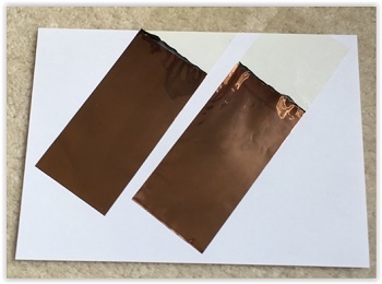
Significant progress has been made over the last few years in building transparent and heat resistant flexible circuits. Several transparent materials were developed along with special manufacturing processes. A copper laminate made from a thin transparent polyimide file plated with a copper layer on both sides for use in traditional manufacturing processes is now available. DKN Research developed a new copper metalizing process using transparent polyimide films. The new laminate will provide manufacturing capabilities using transparent flexible circuits for traditional printed circuit manufacturers.
Polyimide films are the primary substrate material for heat resistant flexible circuits because of the balanced performances between heat resistance and physical properties. The problem is they tend to have an orange or brown color, so the film’s transparency is very low. This is a huge barrier for any optical applications. PET films are another popular substrate material for transparent flexible circuits, but their heat resistance is too low and will not work in standard assembling processes such as soldering and wire bonding. A couple of new heat resistant resins such as LCP have been synthesized and are considered the next generation material for flexible circuits; however, they may not be transparent either. Many chemists used to question the availability of a product that is both transparent and heat resistant. That has changed. Several chemists were successful in synthesizing transparent polyimide resins, and a few companies have brought to market some thin transparent polyimide films that serve as the substrate for heat-resistant flexible circuits.
There are still a few technical hurdles in building transparent flexible circuits. The biggest one is the availability of an appropriate copper laminate for the standard photolithography/chemical etching process. Some of the copper laminates had problems with the surface treatment and gluing of the copper. The transparency of the circuits was remarkably reduced by absorption and scattering.
DKN Research developed a total solutions package for transparent flexible circuits based on each application. During the R&D process, DKN Research has established an electroless and electroplating process of nickel, copper and gold on the transparent polyimide films that provides thin copper laminates available for the standard photolithography/etching process of high density flexible circuits. The new copper laminate could be valuable for traditional flexible circuit manufacturers, because the new laminate does not need any additional equipment or chemicals to build transparent flexible circuits. The transparency of the circuits can be over 85%.
The standard construction of the laminate uses double-sided 3-micron thick copper layers on a 25-micron thick transparent polyimide film. The copper thickness can be thinner at 0.2 microns, and wider thickness ranges will be available for circuit manufacturers. The thin copper conductor could be valuable for semi-additive processes for ultra-fine flexible circuits with microvia holes in the transparent flexible circuits. DKN Research will provide free laminate samples along with a processing guide to circuit manufacturers.
DKN Research will upgrade the laminates and process capabilities to build the leading edge flexible circuits. DKN Research is happy to share the materials and information with circuit manufacturers and device manufacturers. Click here to view a short clip about their products and services.
About DKN Research
DKN Research is a global engineering leader for microelectronics and packaging, specializing in printable & flexible electronics. DKN Research has developed a broad range of leading edge technologies from materials to final devices based on customers’ requirements. They are capable of managing many kinds of materials and manufacturing processes to build and create new devices based on customer needs.
DKN Research provides a broad range of engineering and consulting services not only for the manufacturing community but also the R&D and quality assurance professionals. DKN Research welcomes all inquiries to assist in creating your own circuit devices using its broad range of processing technologies.
Share on:


Testimonial
"Advertising in PCB007 Magazine has been a great way to showcase our bare board testers to the right audience. The I-Connect007 team makes the process smooth and professional. We’re proud to be featured in such a trusted publication."
Klaus Koziol - atgSuggested Items
Episode 6 of Ultra HDI Podcast Series Explores Copper-filled Microvias in Advanced PCB Design and Fabrication
10/15/2025 | I-Connect007I-Connect007 has released Episode 6 of its acclaimed On the Line with... American Standard Circuits: Ultra High Density Interconnect (UHDI) podcast series. In this episode, “Copper Filling of Vias,” host Nolan Johnson once again welcomes John Johnson, Director of Quality and Advanced Technology at American Standard Circuits, for a deep dive into the pros and cons of copper plating microvias—from both the fabricator’s and designer’s perspectives.
Nolan’s Notes: Tariffs, Technologies, and Optimization
10/01/2025 | Nolan Johnson -- Column: Nolan's NotesLast month, SMT007 Magazine spotlighted India, and boy, did we pick a good time to do so. Tariff and trade news involving India was breaking like a storm surge. The U.S. tariffs shifted India from one of the most favorable trade agreements to the least favorable. Electronics continue to be exempt for the time being, but lest you think that we’re free and clear because we manufacture electronics, steel and aluminum are specifically called out at the 50% tariff levels.
MacDermid Alpha & Graphic PLC Lead UK’s First Horizontal Electroless Copper Installation
09/30/2025 | MacDermid Alpha & Graphic PLCMacDermid Alpha Electronics Solutions, a leading supplier of integrated materials and chemistries to the electronics industry, is proud to support Graphic PLC, a Somacis company, with the installation of the first horizontal electroless copper metallization process in the UK.
Electrodeposited Copper Foils Market to Grow by $11.7 Billion Over 2025-2032
09/18/2025 | Globe NewswireThe global electrodeposited copper foils market is poised for dynamic growth, driven by the rising adoption in advanced electronics and renewable energy storage solutions.
MacDermid Alpha Showcases Advanced Interconnect Solutions at PCIM Asia 2025
09/18/2025 | MacDermid Alpha Electronics SolutionsMacDermid Alpha Electronic Solutions, a global leader in materials for power electronics and semiconductor assembly, will showcase its latest interconnect innovations in electronic interconnect materials at PCIM Asia 2025, held from September 24 to 26 at the Shanghai New International Expo Centre, Booth N5-E30