-

- News
- Books
Featured Books
- smt007 Magazine
Latest Issues
Current Issue
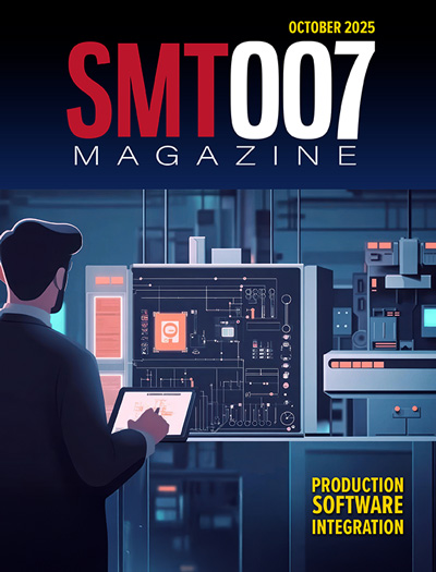
Production Software Integration
EMS companies need advanced software systems to thrive and compete. But these systems require significant effort to integrate and deploy. What is the reality, and how can we make it easier for everyone?

Spotlight on India
We invite you on a virtual tour of India’s thriving ecosystem, guided by the Global Electronics Association’s India office staff, who share their insights into the region’s growth and opportunities.

Supply Chain Strategies
A successful brand is built on strong customer relationships—anchored by a well-orchestrated supply chain at its core. This month, we look at how managing your supply chain directly influences customer perception.
- Articles
- Columns
- Links
- Media kit
||| MENU - smt007 Magazine
How to Streamline PCB Thermal Design
April 1, 2015 | John Parry, Mentor Graphics CorporationEstimated reading time: 2 minutes
Thermal issues with a PCB design are mostly determined during the component selection and layout phases. After this point, only remedial actions are possible if components are found to run too hot. Addressing thermal issues early in PCB design, starting at the system or enclosure level to understand the flow environment critical for air-cooled electronics, can streamline the process. Assumptions about the airflow uniformity in early design that subsequently prove unachievable can have a disastrous effect on the commercial viability of the product and meeting the market window.
Begin Before Placement and Layout
Substantial work can be done well before layout is completed within the electrical design flow. A simple representation of the enclosure can provide information about the air flow profile over the board. Start by smearing the total board power over the total board surface, which will provide a temperature map that will show any hot regions that are caused by a badly distributed air flow. Treat the board as a block with an isotropic conductivity of between 5 W/mK and 10 W/mK to optimize enclosure-level air flow ahead of the PCB design.
Components inject heat locally into the board so the heat flux density into the board below a component will be higher than the average for the board. As a result, the local board temperature will be higher than that predicted in the simulation. Refine the model before using the board temperature to estimate component temperatures. If the board temperature at any point is close to the maximum component case temperature, this limit will be exceeded once the component heat sources are represented discretely.
Guesstimate Component Power
At this stage, make a best-guess estimate of the individual power budgets for the main heat dissipating components that will be used in the design and the approximate size of those packages. This will enable describing them as footprint heat sources in the simulation, smearing the remainder of heat uniformly over the board surface.
Before Selecting the Package, Use 3D Component Models
Include some form of 3D component model in the simulation before the component selection is finalized. By feeding the thermal results back before this milestone is reached, the thermal performance will more likely be considered in the package selection criteria. Some ICs are available in more than one package style, and not all package styles perform equally well from a thermal point of view. The need for a heatsink later may be eliminated by appropriate package selection.
Component temperature, either in the form of a case temperature or junction temperature depending on how the manufacturer has specified the component, is the key measure used to indicate whether the design is thermally acceptable.
Editor's Note: This article originally appeared in the March issue of SMT Magazine.
Testimonial
"Advertising in PCB007 Magazine has been a great way to showcase our bare board testers to the right audience. The I-Connect007 team makes the process smooth and professional. We’re proud to be featured in such a trusted publication."
Klaus Koziol - atgSuggested Items
American Standard Circuits Launches 50th 77-Second Webinar
10/27/2025 | American Standard CircuitsAnaya Vardya, President and CEO of American Standard Circuits/ASC Sunstone Circuits is pleased to announce that they have recently unveiled their 50th 77-second webinar.
Peters, Starteam, and Würth Elektronik Team Up For Digital Coating Technology
10/23/2025 | PetersUnder this heading, the PCB manufacturers Starteam and Würth Elektronik, along with Peters as inkjet coating supplier, have taken the initiative and worked together for months in trusting and target-oriented cooperation, to promote this innovative digital coating technology for solder resists and establish it on the market.
AI Triggers Next Paradigm Shift in PDN
10/23/2025 | Istvan Novak, SamtecArtificial intelligence (AI), together with machine learning (ML), is creating an unprecedented surge of computing and networking infrastructure needs. This, in turn, has dramatically increased the power consumption of computing and networking chips.
SEMICON Japan 2025 to Spotlight Sustainability in AI and Semiconductor Innovation
10/22/2025 | SEMISEMICON Japan 2025, the largest gathering of leaders from the microelectronics manufacturing supply chain in Japan, will bring together more than 1,200 exhibitors showcasing semiconductor solutions from December 17-19 at Tokyo Big Sight.
Zuken Announces ZIW Americas 2026 in Dallas
10/21/2025 | ZukenZuken USA, Inc., a global leader in electrical and electronic design automation, announced Zuken Innovation World (ZIW) Americas 2026, the company’s premier global conference dedicated to advancing the future of electrical and electronic product design. ZIW 2026 will be held June 9-11 in Dallas, Texas.


