


 The Marketing Minute: Staying Positive When the Market Isn’t
 Marcy’s Musings: Continuing to Invent the Future With SEL
 It’s Only Common Sense: Why Failure Is an Opportunity for Growth


Industry 4.0–Inkjet Technology is Changing the World of PCB Manufacturing
March 15, 2017 | Wouter Brok, et al, Meyer Burger B.V.Estimated reading time: 2 minutes
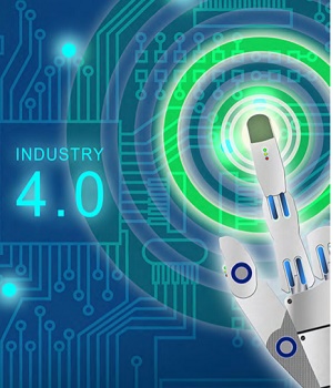
Introduction
When the Germans coined the term Industry 4.0 back in 2011, it wasn’t clear to many what it actually stood for. Although the debate about all the nuances of the term’s meaning is still ongoing, one aspect of it is undisputed: The “computerization of manufacturing” is at the heart of it. Manufacturing techniques throughout many industries continue to become more and more digital. This is also true for PCB manufacturing. Several manufacturing steps offer incredible potential for digitalization. One prime example is the application of solder mask material using industrial inkjet technology.
Solder Mask Printing
The current manufacturing standard for solder mask application involves several process steps which have a significant cost impact:
- Pre-treatment of the PCB
- Full board coating (e.g., curtain coating)
- Artwork film production (photomask)
- UV exposure
- Development
- Post cure
Utilizing state of the art digital inkjet printing for the application of solder mask on PCB boards, the number of process steps can be reduced:
- Pre-treatment of the PCB
- Digital inkjet printing including in situ UV curing
- Post Cure
The benefits of this simplified manufacturing process are obvious. Besides the reduction in required capital equipment and associated labor, the digital process also significantly reduces the use of process chemicals and therefore also the related handling and disposal cost. Overall, the environmental benefits are enormous. Last but not least is the reduction in manufacturing turnaround time—an important asset in to-day’s fast moving electronics business.
Unique Characteristics of Inkjet
Inkjet technology is widely used in homes and offices all over the world for traditional printing applications. Although the fundamental concept of modern industrial inkjet applications is comparable to those printers, there are significant differences. Industrial use of inkjet technology is characterized to a large degree by the type of materials which are deposited. In-stead of traditional ink, materials such as resists, adhesives, conductive inks, polymers and their likes are deposited. Inkjet is a selective coating technology. This means that material is only deposited where it is needed. In the case of solder mask printing, this not only reduces material consumption, but also avoids solder mask material in via holes and other areas where it is difficult to remove or simply not desired. Flushing uncured solder mask material from high aspect ratio holes in the development step is a known challenge in the PCB industry and is completely avoided by inkjet printing.
To read the full version of this article which appeared in the February 2017 issue of The PCB Magazine, click here.
Share on:


Testimonial
"The I-Connect007 team is outstanding—kind, responsive, and a true marketing partner. Their design team created fresh, eye-catching ads, and their editorial support polished our content to let our brand shine. Thank you all! "
Sweeney Ng - CEE PCBSuggested Items
Indium Corporation Promotes Two Leaders in EMEA (Europe, Middle East, and Africa) Markets
08/05/2025 | Indium CorporationWith its commitment to innovation and growth through employee development, Indium Corporation today announced the promotions of Andy Seager to Associate Director, Continental Sales (EMEA), and Karthik Vijay to Senior Technical Manager (EMEA). These advancements reflect their contributions to the company’s continued innovative efforts with customers across Europe, the Middle East, and Africa (EMEA).
MacDermid Alpha Electronics Solutions Unveils Unified Global Website to Deepen Customer, Talent, and Stakeholder Engagement
07/31/2025 | MacDermid Alpha Electronics SolutionsMacDermid Alpha Electronics Solutions, the electronics business of Elements Solutions Inc, today launched macdermidalpha.com - a unified global website built to deepen digital engagement. The launch marks a significant milestone in the business’ ongoing commitment to delivering more meaningful, interactive, and impactful experiences for its customers, talent, and stakeholders worldwide.
KOKI to Showcase Analytical Services and New HF1200 Solder Paste at SMTA Guadalajara 2025
07/31/2025 | KOKIKOKI, a global leader in advanced soldering materials and process optimization services, will exhibit at the SMTA Guadalajara Expo & Tech Forum, taking place September 17 & 18, 2025 at Expo Guadalajara, Salón Jalisco Halls D & E in Guadalajara, Mexico.
Weller Tools Supports Future Talent with Exclusive Donation to SMTA Michigan Student Soldering Competition
07/23/2025 | Weller ToolsWeller Tools, the industry leader in hand soldering solutions, is proud to announce its support of the upcoming SMTA Michigan Expo & Tech Forum by donating a limited-edition 80th Anniversary Black Soldering Set to the event’s student soldering competition.
Koh Young Appoints Tom Hattori as President of Koh Young Japan
07/21/2025 | Koh YoungKoh Young Technology, the global leader in True 3D measurement-based inspection solutions, announced the appointment of Tom Hattori as President of Koh Young Japan (JKY).