


 The Marketing Minute: If Your Marketing Budget Gets Cut in Half, Then What?
 Punching Out: How Are the Big Boys in Electronics Doing?
 It’s Only Common Sense: Complexity Is the Enemy of Profit


Low-Cost Smart Glove Translates American Sign Language Alphabet and Controls Virtual Objects
July 13, 2017 | UC San DiegoEstimated reading time: 3 minutes
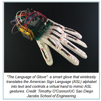
Engineers at the University of California San Diego have developed a smart glove that wirelessly translates the American Sign Language alphabet into text and controls a virtual hand to mimic sign language gestures. The device, which engineers call “The Language of Glove,” was built for less than $100 using stretchable and printable electronics that are inexpensive, commercially available and easy to assemble. The work was published on July 12 in the journal PLOS ONE.
In addition to decoding American Sign Language gestures, researchers are developing the glove to be used in a variety of other applications ranging from virtual and augmented reality to telesurgery, technical training and defense.
“Gesture recognition is just one demonstration of this glove’s capabilities,” said Timothy O’Connor, a nanoengineering Ph.D. student at UC San Diego and the first author of the study. “Our ultimate goal is to make this a smart glove that in the future will allow people to use their hands in virtual reality, which is much more intuitive than using a joystick and other existing controllers. This could be better for games and entertainment, but more importantly for virtual training procedures in medicine, for example, where it would be advantageous to actually simulate the use of one’s hands.”
The glove is unique in that it has sensors made from stretchable materials, is inexpensive and simple to manufacture. “We’ve innovated a low-cost and straightforward design for smart wearable devices using off-the-shelf components. Our work could enable other researchers to develop similar technologies without requiring costly materials or complex fabrication methods,” said Darren Lipomi, a nanoengineering professor who is a member of the Center for Wearable Sensors at UC San Diego and the study’s senior author.
The ‘Language of Glove’
The team built the device using a leather athletic glove and adhered nine stretchable sensors to the back at the knuckles — two on each finger and one on the thumb. The sensors are made of thin strips of a silicon-based polymer coated with a conductive carbon paint. The sensors are secured onto the glove with copper tape. Stainless steel thread connects each of the sensors to a low power, custom-made printed circuit board that’s attached to the back of the wrist.
The sensors change their electrical resistance when stretched or bent. This allows them to code for different letters of the American Sign Language alphabet based on the positions of all nine knuckles. A straight or relaxed knuckle is encoded as “0” and a bent knuckle is encoded as “1”. When signing a particular letter, the glove creates a nine-digit binary key that translates into that letter. For example, the code for the letter “A” (thumb straight, all other fingers curled) is “011111111,” while the code for “B” (thumb bent, all other fingers straight) is “100000000.” Engineers equipped the glove with an accelerometer and pressure sensor to distinguish between letters like “I” and “J”, whose gestures are different but generate the same nine-digit code.
The low power printed circuit board on the glove converts the nine-digit key into a letter and then transmits the signals via Bluetooth to a smartphone or computer screen. The glove can wirelessly translate all 26 letters of the American Sign Language alphabet into text. Researchers also used the glove to control a virtual hand to sign letters in the American Sign Language alphabet.
Moving forward, the team is developing the next version of this glove — one that’s endowed with the sense of touch. The goal is to make a glove that could control either a virtual or robotic hand and then send tactile sensations back to the user’s hand, Lipomi said. “This work is a step toward that direction.”
Related video:
Share on:


Subscribe
Stay ahead of the technologies shaping the future of electronics with our latest newsletter, Advanced Electronics Packaging Digest. Get expert insights on advanced packaging, materials, and system-level innovation, delivered straight to your inbox.
Subscribe now to stay informed, competitive, and connected.
Suggested Items
I-Connect007 Releases The Printed Circuit Designer’s Guide to… Direct Metallization: A Guide to Complex PCB Fabrication
05/13/2026 | I-Connect007As PCB complexity continues to accelerate, fabricators and OEMs are reevaluating long-standing manufacturing processes to meet the demands of AI, HDI, advanced packaging, and next-generation electronics. To address these evolving challenges, I-Connect007 is proud to announce the release of The Printed Circuit Designer’s Guide to… Direct Metallization: A Guide to Complex PCB Fabrication, authored by MacDermid Alpha Solution’s Carmichael Gugliotti.
Driving Innovation: Selecting the Right Laser Source
04/28/2026 | Simon Khesin -- Column: Driving InnovationWhen I first joined Schmoll Maschinen, I brought experience from almost every PCB process, except for laser. As I immersed myself in laser processing, I realized why it can seem so daunting to a newcomer. The complexity arises from three intersecting factors: A vast variety of laser sources: CO2, UV-nano, green-pico, UV-pico, IR-pico, and others; a diverse range of applications: Drilling, cutting, ablation, and more; and an extensive list of materials: These have vastly different absorption rates. Choosing the right machine or laser source is rarely trivial. Even for experienced engineers, answering "Which source is best?" requires examining the business's specific goals.
Institute of Circuit Technology Spring Seminar 2026: A Bright Future in Europe
04/23/2026 | Pete Starkey, I-Connect007Through the leafy lanes and spring flowers of Warwickshire and back to Meridan, the traditional centre of England, and now officially part of the Metropolitan Borough of Solihull in the county of the West Midlands, I attended the Annual General Meeting and Spring Seminar of the Institute of Circuit Technology (ICT) on April 14. Out of the AGM came notable changes in leadership at the top of the Institute: the retirement of Mat Beadel as chair and Emma Hudson as technical director. Effective May 1, Steve Driver is the new chair, and Alun Morgan is the new technical director.
ACCM Unveils Negative and Near-zero CTE Materials for Large-Format AI Chips
04/21/2026 | Advanced Chip and Circuit MaterialsAdvanced Chip and Circuit Materials, Inc. (ACCM) has launched two new materials: Celeritas HM50, with a negative coefficient of thermal expansion (CTE) of -8 ppm/°C to offset the positive CTE and expansion of copper with temperature on circuit boards, and Celeritas HM001, with near-zero CTE and the low-loss performance needed for high-speed signal layers to 224 Gb/s and faster in artificial intelligence (AI) circuits.
Fresh PCB Concepts: Designing PCBs for Harsh Environments—Reliability Is Engineered Upstream
04/23/2026 | Team NCAB -- Column: Fresh PCB ConceptsWhen engineers hear the phrase “harsh environment,” they usually think of the extreme temperature swings, vibration and shock, pressure changes, or radiation in aerospace. However, aerospace is not the only harsh environment where electronic assemblies must survive. Automotive power electronics, downhole oil and gas tools, marine controls, rail systems, defense platforms, and industrial automation equipment all expose PCBs to environments that are equally unforgiving. The stress mechanisms may differ, but the physics does not.