


 Driving Innovation: Mechanical and Optical Processes During Rigid-flex Production
 It’s Only Common Sense: Your Biggest Competitor Is Complacency
 The Chemical Connection: Onshoring PCB Production—Daunting but Certainly Possible


Breaking Electron Waves Provide New Clues to High-Temperature Superconductivity
December 7, 2017 | Brookhaven National LaboratoryEstimated reading time: 4 minutes
Superconductors carry electricity with perfect efficiency, unlike the inevitable waste inherent in traditional conductors like copper. But that perfection comes at the price of extreme cold—even so-called high-temperature superconductivity (HTS) only emerges well below zero degrees Fahrenheit. Discovering the ever-elusive mechanism behind HTS could revolutionize everything from regional power grids to wind turbines.
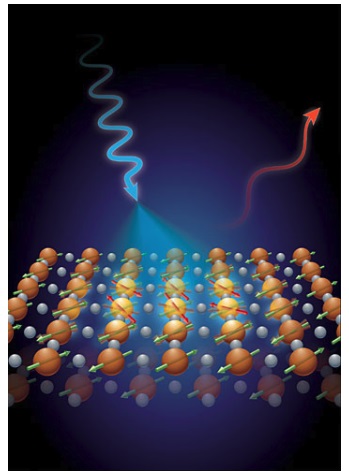
Image caption: In the RIXS technique, intense x-rays deposit energy into the electron waves of atomically thin layers of high-temperature superconductors. The difference in x-ray energy before and after interaction reveals key information about the fundamental behavior of these exciting and mysterious materials.
Now, a collaboration led by the U.S. Department of Energy’s Brookhaven National Laboratory has discovered a surprising breakdown in the electron interactions that may underpin HTS. The scientists found that as superconductivity vanishes at higher temperatures, powerful waves of electrons begin to curiously uncouple and behave independently—like ocean waves splitting and rippling in different directions.
“For the first time, we pinpointed these key electron interactions happening after superconductivity subsides,” said first author and Brookhaven Lab research associate Hu Miao. “The portrait is both stranger and more exciting than we expected, and it offers new ways to understand and potentially exploit these remarkable materials.”
Brookhaven's Robert Konik, Genda Gu, Mark Dean, and Hu Miao
The new study, published November 7 in the journal PNAS, explores the puzzling interplay between two key quantum properties of electrons: spin and charge.
“We know charge and spin lock together and form waves in copper-oxides cooled down to superconducting temperatures,” said study senior author and Brookhaven Lab physicist Mark Dean. “But we didn’t realize that these electron waves persist but seem to uncouple at higher temperatures.”
Electronic stripes and waves
Scientists at Brookhaven Lab discovered in 1995 that spin and charge can lock together and form spatially modulated “stripes” at low temperatures in some HTS materials. Other materials, however, feature correlated electron charges rolling through as charge-density waves that appear to ignore spin entirely. Deepening the HTS mystery, charge and spin can also abandon independence and link together.
“The role of these ‘stripes’ and correlated waves in high-temperature superconductivity is hotly debated,” Miao said. “Some elements may be essential or just a small piece of the larger puzzle. We needed a clearer picture of electron activity across temperatures, particularly the fleeting signals at warmer temperatures.”
Imagine knowing the precise chemical structure of ice, for example, but having no idea what happens as it transforms into liquid or vapor. With these copper-oxide superconductors, or cuprates, there is comparable mystery, but hidden within much more complex materials. Still, the scientists essentially needed to take a freezing-cold sample and meticulously warm it to track exactly how its properties change.
Subtle signals in custom-made materials
The team turned to a well-established HTS material, lanthanum-barium copper-oxides (LBCO) known for strong stripe formations. Brookhaven Lab scientist Genda Gu painstakingly prepared the samples and customized the electron configurations.
“We can’t have any structural abnormalities or errant atoms in these cuprates—they must be perfect,” Dean said. “Genda is among the best in the world at creating these materials, and we’re fortunate to have his talent so close at hand.”
At low temperatures, the electron signals are powerful and easily detected, which is part of why their discovery happened decades ago. To tease out the more elusive signals at higher temperatures, the team needed unprecedented sensitivity.
“We turned to the European Synchrotron Radiation Facility (ESRF) in France for the key experimental work,” Miao said. “Our colleagues operate a beamline that carefully tunes the x-ray energy to resonate with specific electrons and detect tiny changes in their behavior.”
The team used a technique called resonant inelastic x-ray scattering (RIXS) to track position and charge of the electrons. A focused beam of x-rays strikes the material, deposits some energy, and then bounces off into detectors. Those scattered x-rays carry the signature of the electrons they hit along the way.
As the temperature rose in the samples, causing superconductivity to fade, the coupled waves of charge and spin began to unlock and move independently.
“This indicates that their coupling may bolster the stripe formation, or through some unknown mechanism empower high-temperature superconductivity,” Miao said. “It certainly warrants further exploration across other materials to see how prevalent this phenomenon is. It’s a key insight, certainly, but it’s too soon to say how it may unlock the HTS mechanism.”
That further exploration will include additional HTS materials as well as other synchrotron facilities, notably Brookhaven Lab’s National Synchrotron Light Source II (NSLS-II), a DOE Office of Science User Facility.
“Using new beamlines at NSLS-II, we will have the freedom to rotate the sample and take advantage of significantly better energy resolution,” Dean said. “This will give us a more complete picture of electron correlations throughout the sample. There’s much more discovery to come.”
Additional collaborators on the study include Yingying Peng, Giacomo Ghiringhelli, and Lucio Braicovich of the Politecnico di Milano, who contributed to the x-ray scattering, as well as José Lorenzana of the University of Rome, Götz Seibold of the Institute for Physics in Cottbus, Germany, and Robert Konik of Brookhaven Lab, who all contributed to the theory work.
This research was funded by DOE’s Office of Science through Brookhaven Lab’s Center for Emergent Superconductivity.
Share on:


Testimonial
"We’re proud to call I-Connect007 a trusted partner. Their innovative approach and industry insight made our podcast collaboration a success by connecting us with the right audience and delivering real results."
Julia McCaffrey - NCAB GroupSuggested Items
Episode 6 of Ultra HDI Podcast Series Explores Copper-filled Microvias in Advanced PCB Design and Fabrication
10/15/2025 | I-Connect007I-Connect007 has released Episode 6 of its acclaimed On the Line with... American Standard Circuits: Ultra High Density Interconnect (UHDI) podcast series. In this episode, “Copper Filling of Vias,” host Nolan Johnson once again welcomes John Johnson, Director of Quality and Advanced Technology at American Standard Circuits, for a deep dive into the pros and cons of copper plating microvias—from both the fabricator’s and designer’s perspectives.
Nolan’s Notes: Tariffs, Technologies, and Optimization
10/01/2025 | Nolan Johnson -- Column: Nolan's NotesLast month, SMT007 Magazine spotlighted India, and boy, did we pick a good time to do so. Tariff and trade news involving India was breaking like a storm surge. The U.S. tariffs shifted India from one of the most favorable trade agreements to the least favorable. Electronics continue to be exempt for the time being, but lest you think that we’re free and clear because we manufacture electronics, steel and aluminum are specifically called out at the 50% tariff levels.
MacDermid Alpha & Graphic PLC Lead UK’s First Horizontal Electroless Copper Installation
09/30/2025 | MacDermid Alpha & Graphic PLCMacDermid Alpha Electronics Solutions, a leading supplier of integrated materials and chemistries to the electronics industry, is proud to support Graphic PLC, a Somacis company, with the installation of the first horizontal electroless copper metallization process in the UK.
Electrodeposited Copper Foils Market to Grow by $11.7 Billion Over 2025-2032
09/18/2025 | Globe NewswireThe global electrodeposited copper foils market is poised for dynamic growth, driven by the rising adoption in advanced electronics and renewable energy storage solutions.
MacDermid Alpha Showcases Advanced Interconnect Solutions at PCIM Asia 2025
09/18/2025 | MacDermid Alpha Electronics SolutionsMacDermid Alpha Electronic Solutions, a global leader in materials for power electronics and semiconductor assembly, will showcase its latest interconnect innovations in electronic interconnect materials at PCIM Asia 2025, held from September 24 to 26 at the Shanghai New International Expo Centre, Booth N5-E30