


 The Right Approach: Get Ready for ISO 9001 Version 6
 Dan’s Biz Bookshelf: ‘Still Broke: Walmart’s Remarkable Transformation'
 Driving Innovation: Depth Routing Processes—Achieving Unparalleled Precision in Complex PCBs


AT&S Offers Interconnection Tech for Next-Generation 5G Mobile Communications
June 19, 2018 | AT&SEstimated reading time: 2 minutes
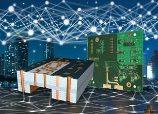
Significantly higher data rates and volumes together with high power densities are resulting in rising requirements for interconnection technologies, too. The new 5G mobile communications generation is undoubtedly an overarching and defining trend here, with applications ranging from infrastructure (base stations) to terminal devices (mobile phones), as well as real-time automation scenarios. AT&S is supporting the current roll-out of the 5G mobile communications generation with high frequency (HF) optimized interconnect solutions and will continue to offer corresponding solutions as the new standard develops.
The launch of the 5G mobile communications generation has far-reaching consequences on the product and system level in terms of miniaturization, functional integration, electromagnetic compatibility (EMC), signal integrity, modularity, safety, security, etc. AT&S therefore analyzed customer requirements and implications for the PCB, substrate and packaging, then initiated and implemented appropriate developments. Innovative solution concepts respond to the challenges of 5G, e.g. using new materials, combining different technologies for hybrid PCB structures, and embedding passive and active circuit components. AT&S invested not only in processes and materials, but also in essential HF measurement equipment to investigate transmission losses, phase shifts and signal delays at up to 100 GHz, for example.
The roll-out of the new 5G mobile communications generation, with frequency bands up to 6 GHz, is already underway. The next step will be to implement 5G millimeter waves with frequencies of 28 GHz or even higher. In principle, for an interconnection technology manufacturer like AT&S, this means reducing signal losses and interference, e.g. by optimizing the dielectric layer in respect of the material (dielectric constant) or thickness, the material transitions (interfaces), or also the copper roughness.
With copper, the major challenge is that while smoother copper offers advantages for HF applications, somewhat greater roughness improves the adhesion of the PCB traces on the basic material. For this reason, AT&S conducted an extensive study of commercially available copper foils for HF applications. The geometry (profile) of the tracks also affects signal delays at higher frequencies and has to be optimized. In addition, AT&S investigated the effects between different metals (copper, gold, nickel) on the skin effect in the GHz range and is developing new surface materials accordingly to get optimized results.
For 5G applications, a hybrid PCB structure combining high-speed layers (HF-optimized) and standard layers represents a performance and cost-optimized solution. AT&S has created a 12-layer hybrid board (HF and FR4 in 2.5D technology) for wireless systems with fully integrated HF antenna. The layers are connected by micro-vias (filled and stacked). Another exemplary HF-optimized solution is a 6-layer board that combines HF layers having a very low dielectric constant with embedded components (application-specific integrated circuits (ASICs) under the antenna structure). The connection between ASICs and antenna is formed by laser-vias.
About AT&S Austria Technologie & Systemtechnik Aktiengesellschaft - First choice for advanced applications
AT&S is the European market leader and one of the globally leading manufacturers of high-end printed circuit boards and IC substrates. AT&S industrialises leading-edge technologies for its core business segments Mobile Devices, Automotive, Industrial and Medical. As an international growth enterprise, AT&S has a global presence with production sites in Austria (Leoben, Fehring) and plants in India (Nanjangud), China (Shanghai, Chongqing) and Korea (Ansan near Seoul). The company employed an average of around 10'000 people in the financial year 2017/18. For further information click here.
Share on:


Testimonial
"Our marketing partnership with I-Connect007 is already delivering. Just a day after our press release went live, we received a direct inquiry about our updated products!"
Rachael Temple - AlltematedSuggested Items
Closing the Loop on PCB Etching Waste
09/09/2025 | Shawn Stone, IECAs the PCB industry continues its push toward greener, more cost-efficient operations, Sigma Engineering’s Mecer System offers a comprehensive solution to two of the industry’s most persistent pain points: etchant consumption and rinse water waste. Designed as a modular, fully automated platform, the Mecer System regenerates spent copper etchants—both alkaline and acidic—and simultaneously recycles rinse water, transforming a traditionally linear chemical process into a closed-loop system.
Driving Innovation: Depth Routing Processes—Achieving Unparalleled Precision in Complex PCBs
09/08/2025 | Kurt Palmer -- Column: Driving InnovationIn PCB manufacturing, the demand for increasingly complex and miniaturized designs continually pushes the boundaries of traditional fabrication methods, including depth routing. Success in these applications demands not only on robust machinery but also sophisticated control functions. PCB manufacturers rely on advanced machine features and process methodologies to meet their precise depth routing goals. Here, I’ll explore some crucial functions that empower manufacturers to master complex depth routing challenges.
Trouble in Your Tank: Minimizing Small-via Defects for High-reliability PCBs
08/27/2025 | Michael Carano -- Column: Trouble in Your TankTo quote the comedian Stephen Wright, “If at first you don’t succeed, then skydiving is not for you.” That can be the battle cry when you find that only small-diameter vias are exhibiting voids. Why are small holes more prone to voids than larger vias when processed through electroless copper? There are several reasons.
The Government Circuit: Navigating New Trade Headwinds and New Partnerships
08/25/2025 | Chris Mitchell -- Column: The Government CircuitAs global trade winds continue to howl, the electronics manufacturing industry finds itself at a critical juncture. After months of warnings, the U.S. Government has implemented a broad array of tariff increases, with fresh duties hitting copper-based products, semiconductors, and imports from many nations. On the positive side, tentative trade agreements with Europe, China, Japan, and other nations are providing at least some clarity and counterbalance.
How Good Design Enables Sustainable PCBs
08/21/2025 | Gerry Partida, Summit InterconnectSustainability has become a key focus for PCB companies seeking to reduce waste, conserve energy, and optimize resources. While many discussions on sustainability center around materials or energy-efficient processes, PCB design is an often overlooked factor that lies at the heart of manufacturing. Good design practices, especially those based on established IPC standards, play a central role in enabling sustainable PCB production. By ensuring designs are manufacturable and reliable, engineers can significantly reduce the environmental impact of their products.