


 It’s Only Common Sense: Marketing Isn’t Fluff, It’s Ammunition
 Driving Innovation: Mechanical and Optical Processes During Rigid-flex Production
 The Chemical Connection: Onshoring PCB Production—Daunting but Certainly Possible


New Material Could Improve Efficiency of Computer Processing and Memory
August 23, 2018 | University of MinnesotaEstimated reading time: 4 minutes
A team of researchers led by the University of Minnesota has developed a new material that could potentially improve the efficiency of computer processing and memory. The researchers have filed a patent on the material with support from the Semiconductor Research Corporation, and people in the semiconductor industry have already requested samples of the material.
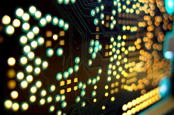
Image caption: This cross-sectional transmission electron microscope image shows a sample used for the charge-to-spin conversion experiment. The nano-sized grains of less than 6 nanometers in the sputtered topological insulator layer created new physical properties for the material that changed the behavior of the electrons in the material. Credit: Wang Group, University of Minnesota
“We used a quantum material that has attracted a lot of attention by the semiconductor industry in the past few years, but created it in unique way that resulted in a material with new physical and spin-electronic properties that could greatly improve computing and memory efficiency,” said lead researcher Jian-Ping Wang, a University of Minnesota Distinguished McKnight Professor and Robert F. Hartmann Chair in electrical engineering.
The new material is in a class of materials called “topological insulators,” which have been studied recently by physics and materials research communities and the semiconductor industry because of their unique spin-electronic transport and magnetic properties. Topological insulators are usually created using a single crystal growth process. Another common fabrication technique uses a process called Molecular Beam Epitaxy in which crystals are grown in a thin film. Both of these techniques cannot be easily scaled up for use in the semiconductor industry.
In this study, researchers started with bismuth selenide (Bi2Se3), a compound of bismuth and selenium. They then used a thin film deposition technique called “sputtering,” which is driven by the momentum exchange between the ions and atoms in the target materials due to collisions. While the sputtering technique is common in the semiconductor industry, this is the first time it has been used to create a topological insulator material that could be scaled up for semiconductor and magnetic industry applications.
However, the fact that the sputtering technique worked was not the most surprising part of the experiment. The nano-sized grains of less than 6 nanometers in the sputtered topological insulator layer created new physical properties for the material that changed the behavior of the electrons in the material. After testing the new material, the researchers found it to be 18 times more efficient in computing processing and memory compared to current materials.
“As the size of the grains decreased, we experienced what we call ‘quantum confinement’ in which the electrons in the material act differently giving us more control over the electron behavior,” said study co-author Tony Low, a University of Minnesota assistant professor of electrical and computer engineering.
Researchers studied the material using the University of Minnesota’s unique high-resolution transmission electron microscopy (TEM), a microscopy technique in which a beam of electrons is transmitted through a specimen to form an image.
“Using our advanced aberration-corrected scanning TEM we managed to identify those nano-sized grains and their interfaces in the film,” said Andre Mkhoyan, a University of Minnesota associate professor of chemical engineering and materials science and electron microscopy expert.
Researchers say this is only the beginning and that this discovery could open the door to more advances in the semiconductor industry as well as related industries, such as magnetic random access memory (MRAM) technology.
“With the new physics of these materials could come many new applications,” said Mahendra DC (Dangi Chhetri), first author of the paper and a physics Ph.D. student in Professor Wang’s lab.
Wang agrees that this cutting-edge research could make a big impact.
“Using the sputtering process to fabricate a quantum material like a bismuth-selenide-based topological insulator is against the intuitive instincts of all researchers in the field and actually is not supported by any existing theory,” Wang said. “Four years ago, with a strong support from Semiconductor Research Corporation and the Defense Advanced Research Projects Agency, we started with a big idea to search for a practical pathway to grow and apply the topological insulator material for future computing and memory devices. Our surprising experimental discovery led to a new theory for topological insulator materials.
“Research is all about being patient and collaborating with team members. This time there was a big pay off,” Wang said.
In addition to Wang, Low, Mkhoyan, and DC, other researchers who were part of the team included University of Minnesota post-doctoral researchers and graduate students Mahdi Jamali, Junyang Chen, Danielle Hickey, Delin Zhang, Zhengyang Zhao, Hongshi Li, Patrick Quarterman, Yang Lv, and associate professor Aurelien Manchon from King Saud University, Saudi Arabia.
This research was funded by the Center for Spintronic Materials, Interfaces and Novel Architectures (C-SPIN) at the University of Minnesota, a Semiconductor Research Corporation program sponsored by the Microelectronics Advanced Research Corp. (MARCO) and the Defense Advanced Research Projects Agency (DARPA). This research used the University of Minnesota College of Science and Engineering Characterization Facility. The research was supported in part by the National Science Foundation through University of Minnesota Materials Research Science and Engineering Center (No. DMR-1420013); and the University of Minnesota College of Science and Engineering’s Minnesota Nano Center supported in part by the National Science Foundation through the NSF through the National Nanotechnology Infrastructure Network (NNIN).
Share on:


Testimonial
"Advertising in PCB007 Magazine has been a great way to showcase our bare board testers to the right audience. The I-Connect007 team makes the process smooth and professional. We’re proud to be featured in such a trusted publication."
Klaus Koziol - atgSuggested Items
SEMI Foundation Honors Applied Materials at SEMICON West with 2025 Excellence in Achievement Award for Talent Development
11/04/2025 | SEMIThe SEMI Foundation announced it recognized Applied Materials, Inc. with the Excellence in Achievement Award at SEMICON West 2025 in Phoenix, Arizona, honoring the company’s outstanding leadership and collaboration in building the next generation of semiconductor talent.
Update: Technica USA Begins Exclusive U.S. Distributor for DCT Cleaning Products
11/03/2025 | Technica USATechnica USA is pleased to announce they have begun shipping product for DCT USA, LLC today. Technica recently announced a strategic partnership as the exclusive master distributor of DCT cleaning products in the United States, which became effective November 1, 2025.
I-Connect007 Editor’s Choice: Five Must-Reads for the Week
10/31/2025 | Nolan Johnson, I-Connect007Last week, the IMPACT conference took place in Taipei, bringing together advanced packaging experts from around the globe to share their knowledge. We’ll be bringing you post-conference coverage over the next few weeks, so look for that in our newsletters, and in the Advanced Electronic Packaging Digest. Other news seemed to have the U.S. at the center of the global discussions. My picks start in Phoenix, where TSMC, NVIDIA, and Amkor are all scrambling to establish new capabilities. There’s nothing like a strong demand signal to cause build-out, and AI chips are doing exactly that.
Real Time with... SMTAI 2025: Navigating Manufacturing Challenges with Akrometrix
11/03/2025 | Real Time with...SMTAIMarcy LaRont and Paul Handler of Aktrometrix share insights from the SMTAI show in Chicago. They address manufacturing challenges, particularly warpage issues, and discuss Akrometrix's solutions. Paul details three optical technologies for measuring warpage and thermal expansion, emphasizing the need for reliability and defect detection in production. The conversation also touches on new industry standards for board warpage, influenced by OEMs.
I-Connect007 Welcomes New Columnist: Leo Lambert, EPTAC
10/30/2025 | I-Connect007I-Connect007 is excited to announce a column by Leo Lambert, an industry veteran with 40 years of experience, an award winner, and technical director at EPTAC. This column, Learning With Leo, will explore the evolution and related challenges of electronics product assembly, especially as it relates to training.