


 The Right Approach: Get Ready for ISO 9001 Version 6
 Dan’s Biz Bookshelf: ‘Still Broke: Walmart’s Remarkable Transformation'
 Driving Innovation: Depth Routing Processes—Achieving Unparalleled Precision in Complex PCBs


Atotech Launches Next Revolution in Electroless Copper for Advanced FPCB
September 3, 2018 | AtotechEstimated reading time: 2 minutes
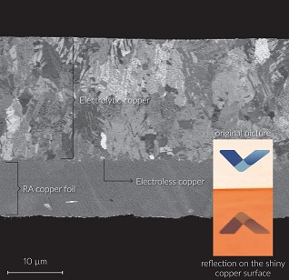
Atotech introduces a new horizontal electroless copper process specifically developed to ensure a blister-free electroless copper deposition and shiny surface appearance after electrolytic copper plating. The new process, Printoganth RA, is compatible with electro-deposited copper (ED), rolled and annealed (RA) as well as “super-flexible RA” (HA) copper foils and best suited to meet OEM requirements for mobile applications.
Image Caption: Printoganth RA – Shiny surface appearance after electrolytic copper plating moderated growth of copper crystals.
RA copper foils are most commonly used for the metallization of next generation flexible substrates. Their special crystal structure, particularly for the “super flexible” HA copper foils, however, requires sophisticated plating solutions in order to achieve the desired surface morphology. One major challenge is the surface appearance after the electrolytic copper plating step. The surface has to have a certain shiny appearance, in order to enable an even etching during structuring and to ensure a reliable automated optical inspection (AOI). In order to overcome this challenge and offer a technically sound solution the Atotech team developed the new Printoganth RA process that complies with different materials when plating advanced flexible and flex-rigid PCBs.
Phenomenal Throwing Power Meets Excellent Coverage with Good Adhesion
Printoganth RA features an excellent coverage on all relevant base materials, including FR4, PI and PI adhesives. A phenomenal throwing power of more than 70% into blind micro vias (BMV) enables good coverage and thicker electroless copper deposits, also at critical spots such as the BMV corners or on exposed adhesive layers within vias. Due to its favorable internal stress characteristics, Printoganth RA allows for an excellent and blister free adhesion of the electroless deposited copper layer even on smooth substrates like PI.
Customer Verification
“Extensive tests at customer sites have confirmed the outstanding performance of Printoganth RA,” states Lars-Eric Pribyl, global product manager for desmear and metallization at Atotech Group. “Already today, two leading manufacturers of FPCBs for next generation smartphones are currently using the Atotech process, which is favored by leading smartphone OEMs. It is the combination of higher process safety thanks to higher throwing power and higher yield rates due to the shiny surface after electroplating that convinced them.”
About Atotech
Atotech is one of the world’s leading manufacturers of specialty chemicals and equipment for the printed circuit board, IC-substrate and semiconductor industries, as well as for the decorative and functional surface finishing industries. Atotech has annual sales of USD1.2 billion (2017). The company is fully committed to sustainability – we develop technologies to minimize waste and to reduce environmental impact. Atotech has its headquarters in Berlin, Germany, and employs about 4,000 people in over 40 countries. For more information, click here.
Share on:


Testimonial
"In a year when every marketing dollar mattered, I chose to keep I-Connect007 in our 2025 plan. Their commitment to high-quality, insightful content aligns with Koh Young’s values and helps readers navigate a changing industry. "
Brent Fischthal - Koh YoungSuggested Items
Closing the Loop on PCB Etching Waste
09/09/2025 | Shawn Stone, IECAs the PCB industry continues its push toward greener, more cost-efficient operations, Sigma Engineering’s Mecer System offers a comprehensive solution to two of the industry’s most persistent pain points: etchant consumption and rinse water waste. Designed as a modular, fully automated platform, the Mecer System regenerates spent copper etchants—both alkaline and acidic—and simultaneously recycles rinse water, transforming a traditionally linear chemical process into a closed-loop system.
Driving Innovation: Depth Routing Processes—Achieving Unparalleled Precision in Complex PCBs
09/08/2025 | Kurt Palmer -- Column: Driving InnovationIn PCB manufacturing, the demand for increasingly complex and miniaturized designs continually pushes the boundaries of traditional fabrication methods, including depth routing. Success in these applications demands not only on robust machinery but also sophisticated control functions. PCB manufacturers rely on advanced machine features and process methodologies to meet their precise depth routing goals. Here, I’ll explore some crucial functions that empower manufacturers to master complex depth routing challenges.
Trouble in Your Tank: Minimizing Small-via Defects for High-reliability PCBs
08/27/2025 | Michael Carano -- Column: Trouble in Your TankTo quote the comedian Stephen Wright, “If at first you don’t succeed, then skydiving is not for you.” That can be the battle cry when you find that only small-diameter vias are exhibiting voids. Why are small holes more prone to voids than larger vias when processed through electroless copper? There are several reasons.
The Government Circuit: Navigating New Trade Headwinds and New Partnerships
08/25/2025 | Chris Mitchell -- Column: The Government CircuitAs global trade winds continue to howl, the electronics manufacturing industry finds itself at a critical juncture. After months of warnings, the U.S. Government has implemented a broad array of tariff increases, with fresh duties hitting copper-based products, semiconductors, and imports from many nations. On the positive side, tentative trade agreements with Europe, China, Japan, and other nations are providing at least some clarity and counterbalance.
How Good Design Enables Sustainable PCBs
08/21/2025 | Gerry Partida, Summit InterconnectSustainability has become a key focus for PCB companies seeking to reduce waste, conserve energy, and optimize resources. While many discussions on sustainability center around materials or energy-efficient processes, PCB design is an often overlooked factor that lies at the heart of manufacturing. Good design practices, especially those based on established IPC standards, play a central role in enabling sustainable PCB production. By ensuring designs are manufacturable and reliable, engineers can significantly reduce the environmental impact of their products.