


 Trouble in Your Tank: Implementing Direct Metallization in Advanced Substrate Packaging
 It’s Only Common Sense: Storytelling That Sells—Stop Pitching, Start Painting Pictures
 The Right Approach: Get Ready for ISO 9001 Version 6


Selective Solder Mask Deposition by Inkjet
February 25, 2019 | Pete Starkey, I-Connect007Estimated reading time: 8 minutes
At IPC APEX EXPO 2019, I spoke with Joost Valeton, product manager for PiXDRO inkjet printing equipment with Meyer Burger, about their newly configured inkjet printer for PCB applications, and bringing awareness to opportunities using selective solder mask deposition.
Pete Starkey: I’m here at IPC APEX EXPO 2019 in San Diego, California, with Joost Valeton from Meyer Burger. Joost, you're launching a new inkjet printer. Is it specifically aimed at the PCB market?
Joost Valeton: In this configuration, yes.
Starkey: Can you give us a brief description of the equipment?
Valeton: Absolutely. At Meyer Burger, we have our JETx platform for volume production. For this specific application—solder mask printing for rigid PCBs—we have defined a configuration for an 18-inch x 24-inch panel size. It comes with the number of print heads and the ink supply we believe is required for this application. It's a new configuration from our well-established product family (Figure 1).
Figure 1: PiXDRO JETx-M, an IPC APEX EXPO 2019 award-winning product.
Starkey: So, this equipment is not new to Meyer Burger. You are experts in producing inkjet equipment and have chosen the characteristics of this particular machine to suit printed circuit application?
Valeton: Exactly. We identified the benefits of doing digital additive manufacturing production of solder mask, and we've looked at the requirements for such a tool in terms of resolution, feature sizes, product size, etc. We've come up with this configuration as a first launching tool in this market. This solution is suited for fast product adjustments and prototyping for PCB manufacturers serving high-tech industries, such as automotive, medical, and aerospace.
Starkey: From your position, are you an equipment supplier and have you cooperated with manufacturers of the consumable materials?
Valeton: Yes. The ink is a huge part of course. As you know, solder mask has specific requirements for the material it has to conform to—not just in color—and for that reason, we work with material suppliers. We mostly work with Agfa from Belgium—who is very close to us, which is convenient—to develop so that we match the performance of the print heads, which for us are also a consumable. We don't build those ourselves; we integrate them. In this case, we have integrated print heads of a well-known supplier. Together with Agfa, we have developed a formulation that matches very well with the characteristics of these print heads.
Starkey: I have been following the development of the market for inkjet printing technology in printed circuit manufacturing for many years. I think that the most difficult objective to realize has been solder mask mainly because solder mask is subject to so many qualifications and standards, customer, and OEM approvals. In my experience, two properties have tended to mutually exclusive. If a formulation were to jet successfully, it would be unlikely to meet qualification requirements. Meanwhile, if it were to meet qualification requirements, it would be unlikely to jet successfully. In the past, a lot of very optimistic claims had been made and then not realized, which made the market a bit apprehensive. But I feel that in the last five years, we've seen a gradual building of confidence in this technology. We have seen several inks reach the stage both of being processable with the equipment and of qualifying to the acceptance standards.
Valeton: Print-head technology has evolved enormously in recent years. Now, with the emergence of silicon MEMS print-head technology, we are finally getting the performance required for demanding applications like solder mask. You're absolutely right that material development has taken a large leap, and we now have a material that can be printed very well and also meets IPC standards on outgassing and all others. The new PiXDRO JETx-M inkjet printer offers unbeatable benefits very specific to these stringent requirements, as smallest droplets of two pL for best-in-class resolution and accuracy eliminate photo and development processes. PiXDRO JETx-M is also environmentally friendly, drastically reducing energy consumption and chemical waste while also conserving water usage (Figure 2).
Figure 2: PiXDRO solder mask best-in-class with smallest droplets.
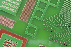
Starkey: Now that I have the opportunity to see some examples of PCBs that have been coated with solder mask using your equipment, perhaps I had been a little complacent in presuming that I understood the current state-of-the-art technology. I've seen examples where you can selectively print in various areas of the PCB while some areas have been left uncoated, with various thicknesses for different purposes, or very fine and high-resolution features.
Valeton: Of course, the benefit of an additive process is the ability to apply the material only where you need it to be. Traditional processes would cover the entire board and remove it just where you don't want it to be. In an additive process, you can apply only where you want it, realizing substantial material savings. As a further bonus of inkjet, by changing the resolution, you can apply various amounts of material across a board in a single print job. For example, if you have a high-voltage application with a high breakdown voltage requirement for your solder mask, you can do that as opposed to the opportunity to save material by printing on other parts of the board where you don't have such stringent requirements. In older techniques, you would need to coat a uniform thickness all over the board (Figure 3).
Furthermore, it gives new possibilities where also I think the industry needs to get an understanding of what this new technology can mean for them such as including different functionalities with a QR code in the solder mask layer for product tracking. Before, it required a separate step because it was not a digital technique. You could not apply it. You would apply solder mask over the entire board so you couldn't even do it in that respect.
Page 1 of 2
Share on:


Testimonial
"The I-Connect007 team is outstanding—kind, responsive, and a true marketing partner. Their design team created fresh, eye-catching ads, and their editorial support polished our content to let our brand shine. Thank you all! "
Sweeney Ng - CEE PCBSuggested Items
Koh Young, Fuji, and Kurtz ERSA Drive Smart Manufacturing Solutions for EV and Automotive Electronics at Kunshan, China Technical Seminar
09/11/2025 | Koh YoungKoh Young Technology, the global leader in True 3D measurement-based inspection solutions, partnered with Fuji Corporation and Kurtz ERSA to host an exclusive technical seminar for leading automotive manufacturers in East China. Held on September 4 at Fuji’s factory in Kunshan, the event gathered participants representing over 35 companies.
MacDermid Alpha Presents at SMTA New Delhi, Bangalore Chapter, on Flux–OSP Interaction
09/09/2025 | MacDermid Alpha Electronics SolutionsMacDermid Alpha contributes technical insights on OSP solderability at the Bangalore Chapter, SMTA reinforcing commitment to knowledge-sharing and industry collaboration.
Electra’s ElectraJet EMJ110 Inkjet Soldermask Now in Black & Blue at Sunrise Electronics
09/08/2025 | Electra Polymers LtdFollowing the successful deployment of Electra’s Green EMJ110 Inkjet Soldermask on KLA’s Orbotech Neos™ platform at Sunrise Electronics in Elk Grove Village, Illinois, production has now moved beyond green.
Absolute EMS: The Science of the Perfect Solder Joint
09/05/2025 | Absolute EMS, Inc.Absolute EMS, Inc., a six-time award-winning provider of fast turnaround, turnkey contract electronic manufacturing services (EMS), is drawing attention to the critical role of 3D Solder Paste Inspection (SPI) in ensuring the reliability of both FLEX and rigid printed circuit board assemblies (PCBAs).
Indium Corporation to Highlight High-Reliability Solder Solutions at SMTA Guadalajara Expo
09/04/2025 | Indium CorporationIndium Corporation, a leading materials refiner, smelter, manufacturer, and supplier to the global electronics, semiconductor, thin-film, and thermal management markets, will feature a range of innovative, high-reliability solder products for printed circuit board assembly (PCBA) at the SMTA Guadalajara Expo and Tech Forum, to be held September 17-18 in Guadalajara, Mexico.