


 The Right Approach: Get Ready for ISO 9001 Version 6
 Dan’s Biz Bookshelf: ‘Still Broke: Walmart’s Remarkable Transformation'
 Driving Innovation: Depth Routing Processes—Achieving Unparalleled Precision in Complex PCBs


Ventec's QMS at German Facility Re-Certified under ISO 9001:2015
May 22, 2019 | Ventec InternationalEstimated reading time: 1 minute
Ventec International Group Co., Ltd. has again achieved ISO 9001:2015 certification for its Quality Management System at its German facility, following an audit by an external certifying authority.
ISO 9001:2015 sets out the criteria for a quality management system and is based on a number of quality management principles including a strong customer focus, the motivation and implication of top management, the process approach and continual improvement. Ventec's facility in Kirchheimbolanden, Germany first achieved ISO 9001:2015 certification in 2016, which, supplements the company's main manufacturing site certifications of AS9100 Rev D for aerospace and IATF 16949:2016 for automotive certifications, and offers customers the highest possible quality standards through a fully controlled global supply chain.
"I am very pleased to receive this re-certification only three years after the first certification—and without any instances of non-conformity," said Frank Lorentz, Internal General Manager. "It recognizes our entire team's hard work and the success of our quality strategy for the benefit of all our customers."
"Ventec maintains robust quality management systems in all its facilities around the world, ensuring that all our customers receive reliable, consistent, good quality products and services from us through our fully controlled global supply chain," said Mark Goodwin, COO Europe & Americas.
About Ventec International Group
Ventec International is a premier supplier to the Global PCB industry. With volume manufacturing facilities in Taiwan and China and distribution locations and manufacturing sites in both the US and Europe, Ventec specializes in advanced copper clad glass reinforced and metal backed substrates. Ventec materials, which include high-quality enhanced FR-4, high-speed/low-loss- & high-performance IMS material technology and an advanced range of thermal management solutions, are manufactured by Ventec using strict quality-controlled processes that are certified to AS9100 Revision D, IATF 16949:2016 and ISO 9001:2015, and are backed by a fully controlled and managed global supply chain, sales- and technical support-network. For more information, visit www.venteclaminates.com.
Visit I-007eBooks to download your copy of Ventec micro eBook today:
The Printed Circuit Designer's Guide to...Thermal Management with Insulated Metal Substrates
Share on:


Testimonial
"Our marketing partnership with I-Connect007 is already delivering. Just a day after our press release went live, we received a direct inquiry about our updated products!"
Rachael Temple - AlltematedSuggested Items
Closing the Loop on PCB Etching Waste
09/09/2025 | Shawn Stone, IECAs the PCB industry continues its push toward greener, more cost-efficient operations, Sigma Engineering’s Mecer System offers a comprehensive solution to two of the industry’s most persistent pain points: etchant consumption and rinse water waste. Designed as a modular, fully automated platform, the Mecer System regenerates spent copper etchants—both alkaline and acidic—and simultaneously recycles rinse water, transforming a traditionally linear chemical process into a closed-loop system.
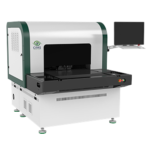
Driving Innovation: Depth Routing Processes—Achieving Unparalleled Precision in Complex PCBs
09/08/2025 | Kurt Palmer -- Column: Driving InnovationIn PCB manufacturing, the demand for increasingly complex and miniaturized designs continually pushes the boundaries of traditional fabrication methods, including depth routing. Success in these applications demands not only on robust machinery but also sophisticated control functions. PCB manufacturers rely on advanced machine features and process methodologies to meet their precise depth routing goals. Here, I’ll explore some crucial functions that empower manufacturers to master complex depth routing challenges.
Trouble in Your Tank: Minimizing Small-via Defects for High-reliability PCBs
08/27/2025 | Michael Carano -- Column: Trouble in Your TankTo quote the comedian Stephen Wright, “If at first you don’t succeed, then skydiving is not for you.” That can be the battle cry when you find that only small-diameter vias are exhibiting voids. Why are small holes more prone to voids than larger vias when processed through electroless copper? There are several reasons.
The Government Circuit: Navigating New Trade Headwinds and New Partnerships
08/25/2025 | Chris Mitchell -- Column: The Government CircuitAs global trade winds continue to howl, the electronics manufacturing industry finds itself at a critical juncture. After months of warnings, the U.S. Government has implemented a broad array of tariff increases, with fresh duties hitting copper-based products, semiconductors, and imports from many nations. On the positive side, tentative trade agreements with Europe, China, Japan, and other nations are providing at least some clarity and counterbalance.
How Good Design Enables Sustainable PCBs
08/21/2025 | Gerry Partida, Summit InterconnectSustainability has become a key focus for PCB companies seeking to reduce waste, conserve energy, and optimize resources. While many discussions on sustainability center around materials or energy-efficient processes, PCB design is an often overlooked factor that lies at the heart of manufacturing. Good design practices, especially those based on established IPC standards, play a central role in enabling sustainable PCB production. By ensuring designs are manufacturable and reliable, engineers can significantly reduce the environmental impact of their products.