


 Driving Innovation: Mechanical and Optical Processes During Rigid-flex Production
 It’s Only Common Sense: Your Biggest Competitor Is Complacency
 The Chemical Connection: Onshoring PCB Production—Daunting but Certainly Possible


Lasers Enable Engineers to Weld Ceramics, No Furnace Required
August 26, 2019 | UC San DiegoEstimated reading time: 2 minutes
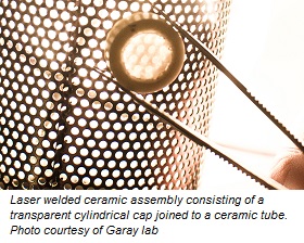
Smartphones that don’t scratch or shatter. Metal-free pacemakers. Electronics for space and other harsh environments. These could all be made possible thanks to a new ceramic welding technology developed by a team of engineers led by the University of California San Diego.
The process uses an ultrafast pulsed laser to melt ceramic materials along the interface and fuse them together. It works in ambient conditions and uses less than 50 watts of laser power, making it more practical than current ceramic welding methods that require heating the parts in a furnace.
Ceramics have been fundamentally challenging to weld together because they need extremely high temperatures to melt, exposing them to extreme temperature gradients that cause cracking, explained senior author Javier E. Garay, a professor of mechanical engineering and materials science and engineering at UC San Diego, who led the work in collaboration with UC Riverside professor and chair of mechanical engineering Guillermo Aguilar. Ceramic materials are of great interest because they are biocompatible, extremely hard and shatter resistant, making them ideal for biomedical implants and protective casings for electronics. However, current ceramic welding procedures are not conducive to making such devices.
“Right now there is no way to encase or seal electronic components inside ceramics because you would have to put the entire assembly in a furnace, which would end up burning the electronics,” Garay said.
Garay, Aguilar and colleagues’ solution was to aim a series of short laser pulses along the interface between two ceramic parts so that heat builds up only at the interface and causes localized melting. They call their method ultrafast pulsed laser welding.
To make it work, the researchers had to optimize two aspects: the laser parameters (exposure time, number of laser pulses, and duration of pulses) and the transparency of the ceramic material. With the right combination, the laser energy couples strongly to the ceramic, allowing welds to be made using low laser power (less than 50 watts) at room temperature. “The sweet spot of ultrafast pulses was two picoseconds at the high repetition rate of one megahertz, along with a moderate total number of pulses. This maximized the melt diameter, minimized material ablation, and timed cooling just right for the best weld possible,” Aguilar said.
“By focusing the energy right where we want it, we avoid setting up temperature gradients throughout the ceramic, so we can encase temperature-sensitive materials without damaging them,” Garay said.
As a proof of concept, the researchers welded a transparent cylindrical cap to the inside of a ceramic tube. Tests showed that the welds are strong enough to hold vacuum.
“The vacuum tests we used on our welds are the same tests that are used in industry to validate seals on electronic and optoelectronic devices,” said first author Elias Penilla, who worked on the project as a postdoctoral researcher in Garay’s research group at UC San Diego.
The process has so far only been used to weld small ceramic parts that are less than two centimeters in size. Future plans will involve optimizing the method for larger scales, as well as for different types of materials and geometries.
Share on:


Testimonial
"The I-Connect007 team is outstanding—kind, responsive, and a true marketing partner. Their design team created fresh, eye-catching ads, and their editorial support polished our content to let our brand shine. Thank you all! "
Sweeney Ng - CEE PCBSuggested Items
Driving Innovation: Mechanical and Optical Processes During Rigid-flex Production
10/28/2025 | Kurt Palmer -- Column: Driving InnovationRigid-flex printed circuit boards are a highly effective solution for placing complex circuitry in tight, three-dimensional spaces. They are now indispensable across a range of industries, from medical devices and aerospace to advanced consumer electronics, helping designers make the most efficient use of available space. However, their unique construction—combining rigid and flexible materials—presents a fundamental challenge for PCB manufacturers.
SMTAI 2025 Review: Reflecting on a Pragmatic and Forward-looking Industry
10/27/2025 | Marcy LaRont, I-Connect007Leaving the show floor on the final afternoon of SMTA International last week in Rosemont, Illinois, it was clear that the show remains a grounded, technically driven event that delivers a solid program, good networking, and an easy space to commune with industry colleagues and meet with customers.
ITW EAE Despatch Ovens Now Support ASTM 5423 Testing
10/15/2025 | ITW EAEAs the demand for high-performance electrical insulation materials continues to grow—driven by the rapid expansion of electric vehicles (EVs) and energy storage systems—thermal processing has become a critical step in material development.
Beyond Thermal Conductivity: Exploring Polymer-based TIM Strategies for High-power-density Electronics
10/13/2025 | Padmanabha Shakthivelu and Nico Bruijnis, MacDermid Alpha Electronics SolutionsAs power density and thermal loads continue to increase, effective thermal management becomes increasingly important. Rapid and efficient heat transfer from power semiconductor chip packages is essential for achieving optimal performance and ensuring long-term reliability of temperature-sensitive components. This is particularly crucial in power systems that support advanced applications such as green energy generation, electric vehicles, aerospace, and defense, along with high-speed computing for data centers and artificial intelligence (AI).
Is Glass Finally Coming of Age?
10/13/2025 | Nolan Johnson, I-Connect007Substrates, by definition, form the base of all electronic devices. Whether discussing silicon wafers for semiconductors, glass-and-epoxy materials in printed circuits, or the base of choice for interposers, all these materials function as substrates. While other substrates have come and gone, silicon and FR-4 have remained the de facto standards for the industry.