


 Driving Innovation: Mechanical and Optical Processes During Rigid-flex Production
 It’s Only Common Sense: Your Biggest Competitor Is Complacency
 The Chemical Connection: Onshoring PCB Production—Daunting but Certainly Possible


Chemists Uncover a Mechanism Behind Doping Organic Semiconductors
September 16, 2019 | University of California - Santa BarbaraEstimated reading time: 3 minutes
Semiconductors — and our mastery of them — have enabled us to develop the technology that underpins our modern society. These devices are responsible for a wide range of electronics, including circuit boards, computer chips and sensors.
The electrical conductance of semiconductors falls between those of insulators, like rubber, and conductors, like copper. By doping the materials with different impurities, scientists can control a semiconductor’s electrical properties. This is what makes them so useful in electronics.
Scientists and engineers have been exploring new types of semiconductors with attractive properties that could result in revolutionary innovations. One class of these new materials is organic semiconductors (OSCs), which are based on carbon rather than silicon. OSCs are lighter and more flexible than their conventional counterparts, properties that lend themselves to all sorts of potential applications, such as flexible electronics, for instance.
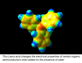
In 2014, UC Santa Barbara’s Professor Thuc-Quyen Nguyen and her lab first reported on doping of OSCs using Lewis acids to increase the conductance of some semiconducting polymers; however, no one knew why this increase happened until now.
Through a collaborative effort, Nguyen and her collages have parsed this mechanism, and their unexpected discovery promises to grant us greater control over these materials. The work was supported by the Department of Energy and the findings appear in the journal Nature Materials.
Researchers at UC Santa Barbara collaborated with an international team from the University of Kentucky, Humboldt University of Berlin and Donghua University in Shanghai. “The doping mechanism using Lewis acids is unique and complex; therefore, it requires a team effort,” Nguyen explained.
“That’s what this paper is all about,” said lead author Brett Yurash, a doctoral candidate in Nguyen’s lab, “figuring out why adding this chemical to the organic semiconductor increases its conductivity.”
“People thought it was just the Lewis acid acting on the organic semiconductor,” he explained. “But it turns out you don’t get that effect unless water is present.”
Apparently, water mediates a key part of this process. The Lewis acid grabs a hydrogen atom from the water and passes it over to the OSC. The extra positive charge makes the OSC molecule unstable, so an electron from a neighboring molecule migrates over to cancel out the charge. This leaves a positively charged “hole” that then contributes to the material’s conductivity.
“The fact that water was having any role at all was really unexpected,” said Yurash, the paper’s lead author.
Most of these reactions are performed in controlled environments. For instance, the experiments at UC Santa Barbara were conducted in dry conditions under a nitrogen atmosphere. There wasn’t supposed to be any humidity in the chamber at all. However, clearly some moisture had made it into the box with the other materials. “Just a tiny amount of water is all it took to have this doping effect,” Yurash said.
Scientists, engineers and technicians need to be able to controllably dope a semiconductor in order for it to be practical. “We’ve totally mastered silicon,” he said. “We can dope it the exact amount we want and it’s very stable.” In contrast, controllably doping OSCs has been a huge challenge.
Lewis acids are actually pretty stable dopants, and the team’s findings apply fairly broadly, beyond simply the few OSCs and acids they tested. Most of the OSC doping work has used molecular dopants Which don’t dissolve readily in many solvents “Lewis acids, on the other hand, are soluble in common organic solvents, cheap, and available in various structures,” Nguyen explained.
Understanding the mechanism at work should enable researchers to purposefully design even better dopants. “This is hopefully going to be the springboard from which more ideas launch,” Yurash said. Ultimately, the team hopes these insights help push organic semiconductors toward broader commercial realization.
Share on:


Testimonial
"Your magazines are a great platform for people to exchange knowledge. Thank you for the work that you do."
Simon Khesin - Schmoll MaschinenSuggested Items
Episode 6 of Ultra HDI Podcast Series Explores Copper-filled Microvias in Advanced PCB Design and Fabrication
10/15/2025 | I-Connect007I-Connect007 has released Episode 6 of its acclaimed On the Line with... American Standard Circuits: Ultra High Density Interconnect (UHDI) podcast series. In this episode, “Copper Filling of Vias,” host Nolan Johnson once again welcomes John Johnson, Director of Quality and Advanced Technology at American Standard Circuits, for a deep dive into the pros and cons of copper plating microvias—from both the fabricator’s and designer’s perspectives.
Nolan’s Notes: Tariffs, Technologies, and Optimization
10/01/2025 | Nolan Johnson -- Column: Nolan's NotesLast month, SMT007 Magazine spotlighted India, and boy, did we pick a good time to do so. Tariff and trade news involving India was breaking like a storm surge. The U.S. tariffs shifted India from one of the most favorable trade agreements to the least favorable. Electronics continue to be exempt for the time being, but lest you think that we’re free and clear because we manufacture electronics, steel and aluminum are specifically called out at the 50% tariff levels.
MacDermid Alpha & Graphic PLC Lead UK’s First Horizontal Electroless Copper Installation
09/30/2025 | MacDermid Alpha & Graphic PLCMacDermid Alpha Electronics Solutions, a leading supplier of integrated materials and chemistries to the electronics industry, is proud to support Graphic PLC, a Somacis company, with the installation of the first horizontal electroless copper metallization process in the UK.
Electrodeposited Copper Foils Market to Grow by $11.7 Billion Over 2025-2032
09/18/2025 | Globe NewswireThe global electrodeposited copper foils market is poised for dynamic growth, driven by the rising adoption in advanced electronics and renewable energy storage solutions.
MacDermid Alpha Showcases Advanced Interconnect Solutions at PCIM Asia 2025
09/18/2025 | MacDermid Alpha Electronics SolutionsMacDermid Alpha Electronic Solutions, a global leader in materials for power electronics and semiconductor assembly, will showcase its latest interconnect innovations in electronic interconnect materials at PCIM Asia 2025, held from September 24 to 26 at the Shanghai New International Expo Centre, Booth N5-E30