


 The Marketing Minute: Marketing With Layers
 The Right Approach: Electro-Tek—A Williams Family Legacy, Part 1
 It’s Only Common Sense: If You’re Not Differentiated, You’re Dead


HENSOLDT and Nano Dimension Achieve Breakthrough in Electronics 3D Printing
May 19, 2020 | Nano DimensionEstimated reading time: 1 minute
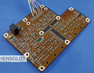
Sensor solutions provider HENSOLDT together with the leading Additively Manufactured Electronics (AME)/Printed Electronics (PE) provider, Nano Dimension, has achieved a major breakthrough on its way to utilizing 3D printing in the development process of high-performance electronics components. Utilizing a newly developed dielectric polymer ink and conductive ink from Nano Dimension, HENSOLDT succeeded in assembling the world-wide first 10-layer printed circuit board (PCB) which carries high-performance electronic structures soldered to both outer sides. Until now, 3D-printed boards could not bear the soldering process necessary for two-sided population of components.
“Military sensor solutions require performance and reliability levels far above those of commercial components.” said HENSOLDT CEO, Thomas Müller. “To have high-density components quickly available with reduced effort by means of 3D printing gives us a competitive edge in the development process of such high-end electronic systems.”
“Nano Dimension’s relationship with HENSOLDT is the type of partnership with customers we are striving for,” commented Yoav Stern, Nano Dimension President and CEO. “Working together and learning from HENSOLDT led us to reach a first-of-its-kind in-depth knowledge of polymer materials applications. Additionally, it guided us in the development of Hi-PEDs (high performance electronic device) that create competitive edges by enabling unique implementations with shortest time to market.”
AMEs are useful to verify a new design and functionality of specialized electronic components before production. AME is a highly agile and individual engineering methodology to prototype a new electronic circuitry. This leads to significant reduction of time and cost in the development process. Furthermore, AME gives a verified and approved design before production starts, leading to higher quality of the final product.
HENSOLDT started working with Nano Dimension’s DragonFly 3D printing system in 2016, in order to examine the possibilities of 3D printing electronics. Last year, HENSOLDT successfully implemented the DragonFly Lights-Out Digital Manufacturing (LDM) printing technology, the industry’s only additive manufacturing platform for round-the-clock 3D printing of electronic circuitry.
Share on:


Testimonial
"Advertising in PCB007 Magazine has been a great way to showcase our bare board testers to the right audience. The I-Connect007 team makes the process smooth and professional. We’re proud to be featured in such a trusted publication."
Klaus Koziol - atgSuggested Items
Foxconn's Rotating CEO, Yang Qiujin, Named One of Asia's Most Influential Women
10/15/2025 | Foxconn ElectronicsHon Hai Precision Industry Co., Ltd.'s management team has once again received recognition! Rotating CEO Kathy Yang has been named to Fortune magazine's " Most Powerful Women Asia 2025 " list of the 100 most influential women in Asia , achieving a remarkable fifth place in her debut.
Light-curable Solutions for Reliable Electronics in Space Applications
10/15/2025 | Virginia Hogan, DymaxDesigning electronics for space environments, particularly those in low Earth orbit (LEO), requires careful consideration of materials that can withstand extreme conditions while supporting long-term reliability. Engineers designing satellite systems, aerospace instrumentation, and high-altitude platforms face a familiar set of challenges: contamination control, mechanical stress, thermal cycling, and manufacturability.
Advanced Semiconductor Packaging Market Sees Rising Adoption Across Automotive and Industrial Sectors
10/14/2025 | openPRThe semiconductor packaging market size is estimated to reach at a CAGR of 7.2% during the forecast period (2024-2031).
Imec Launches 300mm GaN Program to Develop Advanced Power Devices and Reduce Manufacturing Costs
10/13/2025 | ImecImec, a world-leading research and innovation hub in nanoelectronics and digital technologies, welcomes AIXTRON, GlobalFoundries, KLA Corporation, Synopsys, and Veeco as first partners in its 300mm gallium-nitride (GaN) open innovation program track for low- and high-voltage power electronics applications.
NEDME Returns October 22 — The Northwest’s Premier Design & Manufacturing Expo
10/13/2025 | NEDMEThe Northwest Electronics Design & Manufacturing Expo (NEDME) returns on Wednesday, October 22, 2025, at Wingspan Event & Conference Center, Hillsboro. The event brings together engineers, product designers, manufacturers, educators, and community partners for a full day of industry connection, learning, and networking.