


 Dan's Biz Bookshelf: 'Move Your Bus'
 Driving Innovation: Direct Imaging vs. Conventional Exposure
 It’s Only Common Sense: Selling to Today's Generation of Buyers


Isola Opens Expanded R&D and Analytical Laboratory in Arizona
June 19, 2020 | PR NewswireEstimated reading time: 2 minutes
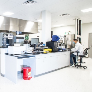
Isola, designer and developer of copper-clad laminates and fabrication materials for multi-layer printed circuit boards (PCBs), has officially opened an expansive R&D and analytical services laboratory at the company's new global headquarters in Chandler, Ariz.
Nearly doubling the size and capacity of the testing facility enables enhanced product development, material qualification, application engineering, and technical support to printed circuit board fabricators and the OEMs they serve. Access to Isola's testing facilities throughout the world is a complimentary service offered to Isola customers. The Arizona operations also include a 118,000-square-foot quick-turnaround manufacturing facility to accommodate the industry's agile demands.
In the R&D and analytical lab, Isola incorporated a refined and optimized workflow with dedicated space for each testing process. These dedicated spaces provide a more optimal working environment for Isola technicians, chemists, and researchers, benefiting customers through enhanced efficiency. The lab's highly trained team conducts electrical, thermal, and mechanical characterizations of resin components and PCB laminate materials used in the production of printed circuit boards and uses advanced test equipment to achieve accurate results in a rapid response environment. Known as the Johann Schumacher Laboratories, the facility is named for an Isola technical fellow and engineer, who—throughout his 35 years with the company—has developed numerous innovations.
"The North American PCB market is all about quick turnaround and high complexity. Isola's investment in local testing and analysis complements the investments our customers have made to meet the growing complexity of the products designed by OEMs," said Travis Kelly, President & CEO. "The expanded R&D and analytical services laboratory furthers our ability to both improve analytical capability and maintain quick turnaround times."
The lab includes a variety of testing equipment—from Fourier Transform Infrared Spectroscopy (FTIR) and Scanning Electron Microscopy (SEM) analysis for identification of contaminants to microsection equipment used for evaluation of printed circuit board integrity after thermal excursions. The thermal analysis area consists of 17 instruments that measure thermal properties as a function of temperature while specimens are subject to a controlled temperature program.
"While thermal analysis is one of the lab's most in-demand services, the global Johann Schumacher Laboratories network, with locations in the U.S., Singapore, and Germany, helps customers work through various challenges related to their products," said Jenny Inocencio, Sr. Manager Global JSL. "Our cross-trained professionals—many of whom also have experience in the manufacturing environment—understand the full process of how materials are assembled, bring keen insights to identifying problems, and confidently consider different approaches. Customers have the advantage of leveraging our global network as their business needs change and during unexpected market events."
Isola's global R&D and analytical laboratory team is led by Ed Kelley, Chief Technology Officer, Phil Whalen, Chief New Product Development and Strategy Officer, Drew Rocha, R&D Manager; and Jenny Inocencio, Senior Manager, Global JSL
Share on:


Suggested Items
The Evolution of Picosecond Laser Drilling
06/19/2025 | Marcy LaRont, PCB007 MagazineIs it hard to imagine a single laser pulse reduced not only from nanoseconds to picoseconds in its pulse duration, but even to femtoseconds? Well, buckle up because it seems we are there. In this interview, Dr. Stefan Rung, technical director of laser machines at Schmoll Maschinen GmbH, traces the technology trajectory of the laser drill from the CO2 laser to cutting-edge picosecond and hybrid laser drilling systems, highlighting the benefits and limitations of each method, and demonstrating how laser innovations are shaping the future of PCB fabrication.
Day 2: More Cutting-edge Insights at the EIPC Summer Conference
06/18/2025 | Pete Starkey, I-Connect007The European Institute for the PCB Community (EIPC) summer conference took place this year in Edinburgh, Scotland, June 3-4. This is the third of three articles on the conference. The other two cover Day 1’s sessions and the opening keynote speech. Below is a recap of the second day’s sessions.
Day 1: Cutting Edge Insights at the EIPC Summer Conference
06/17/2025 | Pete Starkey, I-Connect007The European Institute for the PCB Community (EIPC) Summer Conference took place this year in Edinburgh, Scotland, June 3-4. This is the second of three articles on the conference. The other two cover the keynote speeches and Day 2 of the technical conference. Below is a recap of the first day’s sessions.
Preventing Surface Prep Defects and Ensuring Reliability
06/10/2025 | Marcy LaRont, PCB007 MagazineIn printed circuit board (PCB) fabrication, surface preparation is a critical process that ensures strong adhesion, reliable plating, and long-term product performance. Without proper surface treatment, manufacturers may encounter defects such as delamination, poor solder mask adhesion, and plating failures. This article examines key surface preparation techniques, common defects resulting from improper processes, and real-world case studies that illustrate best practices.
RF PCB Design Tips and Tricks
05/08/2025 | Cherie Litson, EPTAC MIT CID/CID+There are many great books, videos, and information online about designing PCBs for RF circuits. A few of my favorite RF sources are Hans Rosenberg, Stephen Chavez, and Rick Hartley, but there are many more. These PCB design engineers have a very good perspective on what it takes to take an RF design from schematic concept to PCB layout.