


 Dan’s Biz Bookshelf: ‘The Next RenAIssance: AI and the Expansion of Human Potential’
 The Chemical Connection: When the Industry Moves Faster Than the Standards
 Driving Innovation: Selecting the Right Laser Source


Kuprion Introduces ActiveCopper Filled Thermal Vias
February 12, 2021 | Kuprion, Inc.Estimated reading time: 2 minutes
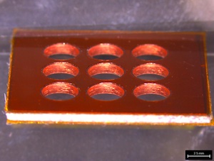
Kuprion, Inc., a spinout of Lockheed Martin, has introduced ActiveCopper™ Filled Thermal Vias, leveraging a patented technology breakthrough that addresses the increased reliability demands of heat and power dissipation for complex, advanced high performance systems.
Lead-free and RoHs-compliant, ActiveCopper is a flowable, engineered copper paste—a dense and sticky form of copper, which is safe to handle in air. To enhance heat and power dissipation, ActiveCopper Filled Thermal Vias provide a more efficient heat dissipation path directly incorporated into PCBs with placement directly under a surface-mounted IC ‘heat source’ that allows direct surface mount bonding for maximum heat transfer using Kuprion’s surface mount copper material. Placing the large 3-5mm diameter thermal vias directly underneath an IC allows direct bonding to such a via, and enables significant reduction in thermal resistance. This facilitates efficient heat dissipation not only on the top surface, but through the PCB to the back side.
“The heat generated by integrated circuits poses great challenges, especially given today’s faster speeds, reduced board real estate and the multitude of devices being populated on PCBs. These demands require more efficient methods of heat and power dissipation to ensure product performance and life for increasingly complex electronic systems,” stated Nick Antonopoulos, CEO at Kuprion. “The PCB by nature, like common FR4 material, is not a good thermal conductor. It’s made of substrate materials that are insulating electrical interconnections between components, but ActiveCopper Filled Thermal Vias provides an ideal solution.”
Kuprion’s Active Cu (ActiveCopper) Thermal Via paste is easily applied by printing, or squeegeeing into these vias, where it is converted into bulk copper during processing. This allows for thermal conductivity of at least 150 W m-1 K-1, and fills holes from micro vias to 4+ mm diameter vias while sintering at approximately 200°C. Additionally, there is no re-melting after sintering, allowing for unlimited reflow sequences.
ActiveCopper Filled Thermal Vias are ideal for advanced high power/high performance applications such as 5G transreceivers/power amplifiers, industrial LEDs, graphics cards, data servers, routers, and automotive lighting with the following advantages:
- Lead-free, RoHs-compliant; nearly 100 percent densified bulk copper after sintering
- No re-melting after sintering; converts to bulk copper (m.p. 1084°C)
- Enables unlimited reflow sequences
- Thermal conductivity: 150 - 160 W m-1 K-1
- Rapid processing: 20 - 40 minutes; no-clean material system
- Proven solution backed by 12+ years of R&D
- Cost-effective and ready for immediate use for a range of global customer applications
Share on:


Testimonial
"Advertising in PCB007 Magazine has been a great way to showcase our bare board testers to the right audience. The I-Connect007 team makes the process smooth and professional. We’re proud to be featured in such a trusted publication."
Klaus Koziol - atgSuggested Items
Driving Innovation: Selecting the Right Laser Source
04/28/2026 | Simon Khesin -- Column: Driving InnovationWhen I first joined Schmoll Maschinen, I brought experience from almost every PCB process, except for laser. As I immersed myself in laser processing, I realized why it can seem so daunting to a newcomer. The complexity arises from three intersecting factors: A vast variety of laser sources: CO2, UV-nano, green-pico, UV-pico, IR-pico, and others; a diverse range of applications: Drilling, cutting, ablation, and more; and an extensive list of materials: These have vastly different absorption rates. Choosing the right machine or laser source is rarely trivial. Even for experienced engineers, answering "Which source is best?" requires examining the business's specific goals.
Institute of Circuit Technology Spring Seminar 2026: A Bright Future in Europe
04/23/2026 | Pete Starkey, I-Connect007Through the leafy lanes and spring flowers of Warwickshire and back to Meridan, the traditional centre of England, and now officially part of the Metropolitan Borough of Solihull in the county of the West Midlands, I attended the Annual General Meeting and Spring Seminar of the Institute of Circuit Technology (ICT) on April 14. Out of the AGM came notable changes in leadership at the top of the Institute: the retirement of Mat Beadel as chair and Emma Hudson as technical director. Effective May 1, Steve Driver is the new chair, and Alun Morgan is the new technical director.
ACCM Unveils Negative and Near-zero CTE Materials for Large-Format AI Chips
04/21/2026 | Advanced Chip and Circuit MaterialsAdvanced Chip and Circuit Materials, Inc. (ACCM) has launched two new materials: Celeritas HM50, with a negative coefficient of thermal expansion (CTE) of -8 ppm/°C to offset the positive CTE and expansion of copper with temperature on circuit boards, and Celeritas HM001, with near-zero CTE and the low-loss performance needed for high-speed signal layers to 224 Gb/s and faster in artificial intelligence (AI) circuits.
Fresh PCB Concepts: Designing PCBs for Harsh Environments—Reliability Is Engineered Upstream
04/23/2026 | Team NCAB -- Column: Fresh PCB ConceptsWhen engineers hear the phrase “harsh environment,” they usually think of the extreme temperature swings, vibration and shock, pressure changes, or radiation in aerospace. However, aerospace is not the only harsh environment where electronic assemblies must survive. Automotive power electronics, downhole oil and gas tools, marine controls, rail systems, defense platforms, and industrial automation equipment all expose PCBs to environments that are equally unforgiving. The stress mechanisms may differ, but the physics does not.
Advanced Packaging for AI: Reliability Starts at the Cu/Cu/Cu Microvia Junction
04/20/2026 | Kuldip Johal, MKS' AtotechThe rapid growth of AI computing, from training clusters to inference at scale, is reshaping demand across the entire electronics supply chain. Advances in technology requirements, such as higher bandwidth, lower latency, and greater compute density, are driving the development of advanced packaging technologies and transforming the PCB industry across design, manufacturing, testing, and even architecture.