


 Driving Innovation: Direct Imaging vs. Conventional Exposure
 It’s Only Common Sense: Selling to Today's Generation of Buyers
 Dan’s Biz Bookshelf: ‘Believe in Better'


Avicena Raises $25M in Series A to Fund Development of High Capacity microLED-based Optical Interconnects
August 2, 2022 | Business WireEstimated reading time: 1 minute
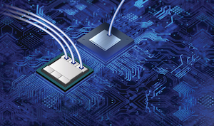
AvicenaTech Corp., the leader in microLED-based chip-to-chip interconnects, announced that the company has secured $25M in Series A funding from Samsung Catalyst Fund, Cerberus Capital Management, Clear Ventures, and Micron Ventures to drive the development of products based on Avicena’s breakthrough photonic I/O solution.
“We believe that Avicena technology can be transformational in unlocking compute-to-memory chip-to-chip high-speed interconnects. Such technology can be central to supporting future disaggregated architectures and distributed high-performance computing (HPC) systems,” said Marco Chisari, EVP of Samsung Electronics and Head of the Samsung Semiconductor Innovation Center.
“We are excited to participate in this round at Avicena,” said Amir Salek, Senior Managing Director at Cerberus Capital Management and former Head of Silicon for Google Infrastructure and Cloud. “Avicena has a highly differentiated technology addressing one of the main challenges in modern computer architecture. The technology offered by Avicena meets the needs for scaling future HPC and cloud compute networks and covers applications in conventional datacenter and 5G cellular networking.”
Avicena’s LightBundleTM I/O solution eliminates the existing bottlenecks of copper links triggered by power consumption, latency, reach and bandwidth density thus dramatically improving existing system performance. This enables new, dramatically higher-performing architectures in artificial intelligence (AI), machine learning (ML), cloud computing, next generation cellular radio, remote sensing, and aerospace applications.
The groundbreaking LightBundleTM technology is based on arrays of GaN micro-emitters that leverage the microLED display ecosystem and can be integrated onto any high-performance CMOS IC. Avicena leverages recent advances in the display industry to enable high volume, low-cost production of highly optimized microLED arrays.
“Avicena’s differentiated interconnect technology promises to enable next-generation high-performance processor and memory clusters,” said Gayathri Radhakrishnan, Senior Director at Micron Ventures. “Avicena represents a strategic investment opportunity for Micron Technology to support innovation in HPC architectures with our partners and customers.”
“We are excited about closing our Series A funding with a distinguished group of existing and new investors,” said Bardia Pezeshki, Founder and CEO of Avicena. “We will use the new funds to scale our team and build initial products for our growing family of partners and customers.”
Share on:


Suggested Items
The Evolution of Picosecond Laser Drilling
06/19/2025 | Marcy LaRont, PCB007 MagazineIs it hard to imagine a single laser pulse reduced not only from nanoseconds to picoseconds in its pulse duration, but even to femtoseconds? Well, buckle up because it seems we are there. In this interview, Dr. Stefan Rung, technical director of laser machines at Schmoll Maschinen GmbH, traces the technology trajectory of the laser drill from the CO2 laser to cutting-edge picosecond and hybrid laser drilling systems, highlighting the benefits and limitations of each method, and demonstrating how laser innovations are shaping the future of PCB fabrication.
Day 2: More Cutting-edge Insights at the EIPC Summer Conference
06/18/2025 | Pete Starkey, I-Connect007The European Institute for the PCB Community (EIPC) summer conference took place this year in Edinburgh, Scotland, June 3-4. This is the third of three articles on the conference. The other two cover Day 1’s sessions and the opening keynote speech. Below is a recap of the second day’s sessions.
Day 1: Cutting Edge Insights at the EIPC Summer Conference
06/17/2025 | Pete Starkey, I-Connect007The European Institute for the PCB Community (EIPC) Summer Conference took place this year in Edinburgh, Scotland, June 3-4. This is the second of three articles on the conference. The other two cover the keynote speeches and Day 2 of the technical conference. Below is a recap of the first day’s sessions.
Preventing Surface Prep Defects and Ensuring Reliability
06/10/2025 | Marcy LaRont, PCB007 MagazineIn printed circuit board (PCB) fabrication, surface preparation is a critical process that ensures strong adhesion, reliable plating, and long-term product performance. Without proper surface treatment, manufacturers may encounter defects such as delamination, poor solder mask adhesion, and plating failures. This article examines key surface preparation techniques, common defects resulting from improper processes, and real-world case studies that illustrate best practices.
RF PCB Design Tips and Tricks
05/08/2025 | Cherie Litson, EPTAC MIT CID/CID+There are many great books, videos, and information online about designing PCBs for RF circuits. A few of my favorite RF sources are Hans Rosenberg, Stephen Chavez, and Rick Hartley, but there are many more. These PCB design engineers have a very good perspective on what it takes to take an RF design from schematic concept to PCB layout.