


 Trouble in Your Tank: Organic Addition Agents in Electrolytic Copper Plating
 It’s Only Common Sense: Selling During an Economic Downturn
 Marcy’s Musings: Can You Hear the Voices?


Eighteen New Semiconductor Fabs to Start Construction in 2025
January 8, 2025 | SEMIEstimated reading time: 2 minutes
The semiconductor industry is expected to start 18 new fab construction projects in 2025*, according to SEMI’s latest quarterly World Fab Forecast report. The new projects include three 200mm and fifteen 300mm facilities, the majority of which are expected to begin operations from 2026 to 2027.
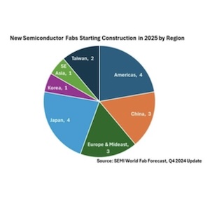
In 2025, the Americas and Japan are the leading regions with four projects each. The China and Europe & Middle East regions are each tied for third place with three planned construction projects. Taiwan has two planned projects, while Korea and Southeast Asia have one project each for 2025.
“The semiconductor industry has reached a pivotal juncture, with investments driving both leading-edge and mainstream technologies to meet evolving global demands,” said Ajit Manocha, SEMI President and CEO. “Generative AI and high-performance computing are fueling advancements in the leading-edge logic and memory segments, while mainstream nodes continue to underpin critical applications in automotive, IoT and power electronics. The construction of 18 new semiconductor fabs set to begin in 2025 demonstrates the industry’s commitment to support innovation and significant economic growth.”
Covering 2023 to 2025, the 4Q 2024 edition of World Fab Forecast report shows that the global semiconductor industry plans to begin operation of 97 new high-volume fabs. This includes 48 projects in 2024 and 32 projects set to launch in 2025, with wafer sizes ranging from 300mm to 50mm.
Advanced Nodes Lead Semiconductor Industry Expansion
Semiconductor capacity is projected to further accelerate, with a 6.6% yearly growth rate forecast to total 33.6 million wafers per month (wpm)** for 2025. This expansion will be primarily driven by leading-edge logic technologies in high-performance computing (HPC) applications and the increasing penetration of generative AI in edge devices.
The semiconductor industry is intensifying efforts to build advanced computing capabilities, responding to the escalating computational demands of large language models (LLMs). Chip manufacturers are aggressively expanding advanced node capacities (7nm and below), which are expected to see an industry-leading 16% yearly growth rate for an increase of more than 300,000 wpm to total 2.2 million wpm in 2025.
Boosted by China’s chip self-sufficiency strategy and expected demand from automotive and IoT applications, mainstream nodes (8nm~45nm) are predicted to add another 6% capacity, surpassing the 15 million wpm milestone in 2025.
Mature technology nodes (50nm and above) are experiencing a more conservative expansion, reflecting the market’s slow recovery and low utilization rates. This segment is expected to grow 5%, reaching 14 million wpm in 2025.
Foundry Segment Continues Strong Capacity Growth
Foundry suppliers are expected to remain the leaders in semiconductor equipment purchases. The Foundry segment is projected to increase capacity by 10.9% year-over-year, rising from 11.3 million wpm in 2024 to a record 12.6 million wpm in 2025.
The overall memory segment shows a measured capacity expansion, with modest growth of 3.5% in 2024 and 2.9% in 2025. However, strong generative AI demand is driving significant changes in memory markets. High-bandwidth memory (HBM) is experiencing a notable surge, creating divergent capacity growth trends between the DRAM and NAND flash segments.
The DRAM segment is expected to maintain robust growth, projecting approximately a 7% year-over-year increase to 4.5 million wpm in 2025. Conversely, the installed capacity for 3D NAND is anticipated to grow 5%, reaching 3.7 million wpm in the same period.
The latest update of the SEMI World Fab Forecast report, published in December 2024, lists more than 1,500 facilities and lines globally, including 180 volume facilities and lines with various probabilities expected to start operation in 2025 or later.
Share on:


Suggested Items
TRI at SMTA Wisconsin Expo 2025
04/24/2025 | TRITest Research, Inc. (TRI), the leading test and inspection systems provider for the electronics manufacturing industry, will join the SMTA Wisconsin Expo 2025.
Driving Sustainability in PCB Design
04/24/2025 | Marcy LaRont, I-Connect007Filbert (Fil) Arzola is an electrical engineer at Raytheon. He’s smart, entertaining, and passionate about PCB design. As it turns out, he’s also passionate about “Mother Earth,” as he calls her. Born and raised in Southern California, he freely admits that he turns the water off when he brushes his teeth and yells at his brother for throwing batteries in the garbage. But when looking at the issue of sustainability and PCB design, he urges his audiences to ponder what sustainability looks like. Can PCB designers, he asks, make any impact on sustainability at all?
Real Time with... IPC APEX EXPO: Silicon Geometry's Signal Integrity Impact on PCBs
04/24/2025 | Marcy LaRont, I-Connect007At IPC APEX EXPO 2025, Kris Moyer addressed the importance of understanding the impact of silicon geometry reduction on signal integrity and PCB performance. Kris says signal integrity considerations are necessary for so many designs today, regardless of clock frequency. He discusses valuable insights from attendees regarding embedded resistor technology and the effects of radiation on smaller silicon features in aerospace applications.
Recognizing the IPC Committee Volunteer Awards in 2025
04/24/2025 | Patty Goldman, I-Connect007In 2023, IPC created two new awards to honor standards development committee volunteers: The Hillman-Lambert Award for Volunteer of the Year and the Kessler-Goldman Award for Committee Leader of the Year. The awards were named after Hall of Fame members whose service to standards development is well-known and who have demonstrated the skills and principles that the awardees should also have.
Explore Thermal Management Solutions in Latest Podcast Series—New Episode Now Available
04/23/2025 | I-Connect007I-Connect007 is excited to share the latest episode in our new podcast series! In this episode, Ryan returns to discuss practical strategies for managing heat, starting early in the design planning and specification phases. After all, prevention means there’s less to mitigate later.