


 The Marketing Minute: Cracking the Code of Technical Marketing
 Trouble in Your Tank: Implementing Direct Metallization in Advanced Substrate Packaging


First Solar Cell Made of Highly Ordered Molecular Frameworks
June 22, 2015 | Karlsruhe Institute of Technology (KIT)Estimated reading time: 3 minutes
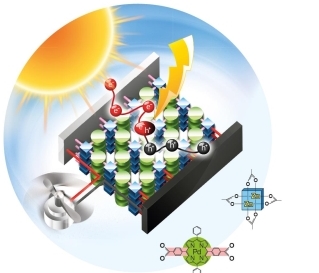
Researchers at KIT have developed a material suited for photo-voltaics. For the first time, a functioning organic solar cell con-sisting of a single component has been produced on the basis of metal-organic framework compounds (MOFs). The material is highly elastic and might also be used for the flexible coating of clothes and deformable components. This development success is presented on the front page of the journal Angewandte Chemie International Edition.
“We have opened the door to a new room,” says Professor Christof Wöll, Director of KIT Institute of Functional Interfaces (IFG). “This new application of metal-organic framework compounds is the be-ginning only. The end of this development line is far from being reached,” the physicist emphasizes.
Metal-organic frameworks, briefly called MOFs, consist of two basic elements, metal node points and organic molecules, which are assembled to form microporous, crystalline materials. For about a decade, MOFs have been attracting considerable interest of re-searchers, because their functionality can be adjusted by varying the components. “A number of properties of the material can be changed,” Wöll explains. So far, more than 20,000 different MOF types have been developed and used mostly for the storage or separation of gases.
The team of scientists under the direction of KIT has now produced MOFs based on porphyrines. These porphyrine-based MOFs have highly interesting photophysical properties: Apart from a high effi-ciency in producing charge carriers, a high mobility of the latter is observed. Computations made by the group of Professor Thomas Heine from Jacobs University Bremen, which is also involved in the project, suggest that the excellent properties of the solar cell result from an additional mechanism – the formation of indirect band gaps – that plays an important role in photovoltaics. Nature uses porphy-rines as universal molecules e.g. in hemoglobin and chlorophyll, where these organic dyes convert light into chemical energy. A met-al-organic solar cell produced on the basis of this novel porphyrine-MOF is now presented by the researchers in the journal Angewandte Chemie (Applied Chemistry). The contribution is entitled “Photoinduzierte Erzeugung von Ladungsträgern in epitaktischen MOF-Dünnschichten: hohe Leistung aufgrund einer indirekten elekt-ronischen Bandlücke?“ (photo-induced generation of charge carriers in epitactic MOF-thin layers: high efficiency resulting from an indirect electronic band gap?).
“The clou is that we just need a single organic molecule in the solar cell,” Wöll says. The researchers expect that the photovoltaic capac-ity of the material may be increased considerably in the future by filling the pores in the crystalline lattice structure with molecules that can release and take up electric charges.
By means of a process developed at KIT, the crystalline frameworks grow in layers on a transparent, conductive carrier surface and form a homogeneous thin film, so-called SURMOFs. “The SURMOF process is suited in principle for a continuous manufacturing process and also allows for the coating of larger plastic carrier surfaces,” Wöll says. Thanks to their mechanical properties, MOF thin films of a few hundred nanometers in thickness can be used for flexible solar cells or for the coating of clothing material or deformable components. While the demand for technical systems converting sunlight into electricity is increasing, organic materials represent a highly interesting alternative to silicon that has to be processed at high costs before it can be used for the photoactive layer of a solar cell.
About Karlsruhe Institute of Technology (KIT)
Karlsruhe Institute of Technology (KIT) is a public corporation pursuing the tasks of a state university of Baden-Wuerttemberg and of a national research center of the Helmholtz Association. The KIT mission combines the three core tasks of research, higher education, and innovation. With about 9,400 employees and 24,500 students, KIT is one of the big institutions of research and higher education in natural sciences and engineering in Europe.
Share on:


Testimonial
"The I-Connect007 team is outstanding—kind, responsive, and a true marketing partner. Their design team created fresh, eye-catching ads, and their editorial support polished our content to let our brand shine. Thank you all! "
Sweeney Ng - CEE PCBSuggested Items
Alternative Manufacturing, Inc. (AMI) Announces Commitment to Excellence in Industrial, Defense, Aerospace, Renewables, and Robotics Markets
09/16/2025 | Alternative Manufacturing, Inc.Alternative Manufacturing, Inc. (AMI), a 100% employee-owned contract manufacturer, proudly reaffirms its leadership in the electronics manufacturing services (EMS) industry with a continued commitment to delivering high-quality PCBAs and box builds across the industrial, defense, aerospace, renewable energy, and robotics markets.
Sustainability and Selective Soldering
09/15/2025 | Dr. Samuel J. McMaster, Pillarhouse InternationalSustainability is more than just a buzzword for the electronics industry; it’s a key goal for all manufacturing processes. This is more than a box-ticking exercise or simply doing a small part for environmentally friendly processes. Moving toward sustainable solutions drives innovation and operational efficiency.
Trouble in Your Tank: Implementing Direct Metallization in Advanced Substrate Packaging
09/15/2025 | Michael Carano -- Column: Trouble in Your TankDirect metallization systems based on conductive graphite are gaining popularity throughout the world. The environmental and productivity gains achievable with this process are outstanding. Direct metallization reduces the costs of compliance, waste treatment, and legal issues related to chemical exposure. A graphite-based direct plate system has been devised to address these needs.
EV Group Achieves Breakthrough in Hybrid Bonding Overlay Control for Chiplet Integration
09/12/2025 | EV GroupEV Group (EVG), a leading provider of innovative process solutions and expertise serving leading-edge and future semiconductor designs and chip integration schemes, today unveiled the EVG®40 D2W—the first dedicated die-to-wafer overlay metrology platform to deliver 100 percent die overlay measurement on 300-mm wafers at high precision and speeds needed for production environments. With up to 15X higher throughput than EVG’s industry benchmark EVG®40 NT2 system designed for hybrid wafer bonding metrology, the new EVG40 D2W enables chipmakers to verify die placement accuracy and take rapid corrective action, improving process control and yield in high-volume manufacturing (HVM).
Integrating Uniplate PLBCu6 With the Digital Factory Suite
09/12/2025 | Giovanni Obino and Andreas Schatz, MKS' AtotechPrinted circuit board manufacturing is rapidly changing, driven by miniaturization, stringent reliability requirements, and growing pressure for sustainable production. Meeting these challenges requires more than incremental improvements; it demands a combination of precise equipment and real-time process intelligence. The pairing of Uniplate® PLBCu6 with the Digital Factory Suite (DFS) demonstrates how hardware and software can work together to create more responsive, resource-efficient manufacturing.