


 The Marketing Minute: Staying Positive When the Market Isn’t
 Marcy’s Musings: Continuing to Invent the Future With SEL
 It’s Only Common Sense: Why Failure Is an Opportunity for Growth


All About Flex: Process Controls for Flexible Circuit Fabrication
December 17, 2015 | Dave Becker, All FlexEstimated reading time: 1 minute
Manufacturers of flexible circuits use several chemical processes for fabrication. These processes are generally located in a common area of the plant because of facility requirements and environmental considerations. These chemical operations are referred to as wet processes. Some of the specific processes that would be characterized as wet process in circuit fabrication:
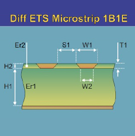
• Develop-etch-strip: Photosensitive resist is developed so the unneeded resist is washed away, leaving a pattern of resist that defines the circuitry. The subsequent etching operation removes the base metal (normally copper) that has been exposed by the patterned resist. The last step is to remove (strip away) the resist that defined the circuitry.
• Copper plating: This is typically an electro-chemical operation. Metal is electrodeposited onto the base metal surface thereby creating a thin, robust coating. Electroplating of copper is the most common example and is used to create electrical connection between traces on the top and bottom of the insulating dielectric film.
• Shadow plating: A laminate of metal-dielectric-metal is initially drilled, punched, or laser ablated to form the vias. In order to initially create an electrical connection between the layers of metal, the dielectric must be coated with a conductive material. Shadow plating coats graphite inside a via and is a chemical process commonly used by flexible circuit manufacturers.
Each of these operations relies on chemical reactions, which may be supplemented with mechanical agitation, temperature and voltage/current. In most cases the chemical makeup is the most critical element that affects the output. It is vital that critical process parameters are tightly controlled to assure desired results. The following are the basic outputs that are monitored and compared to a process or customer specification:
- Trace width and spacing
- Metal thickness
- Via integrity
- Metal composition
To read the full article click here.
Editor's Note: This article originally appeared in the November 2015 issue of The PCB Magazine.
Share on:


Testimonial
"Our marketing partnership with I-Connect007 is already delivering. Just a day after our press release went live, we received a direct inquiry about our updated products!"
Rachael Temple - AlltematedSuggested Items
How Good Design Enables Sustainable PCBs
08/21/2025 | Gerry Partida, Summit InterconnectSustainability has become a key focus for PCB companies seeking to reduce waste, conserve energy, and optimize resources. While many discussions on sustainability center around materials or energy-efficient processes, PCB design is an often overlooked factor that lies at the heart of manufacturing. Good design practices, especially those based on established IPC standards, play a central role in enabling sustainable PCB production. By ensuring designs are manufacturable and reliable, engineers can significantly reduce the environmental impact of their products.
50% Copper Tariffs, 100% Chip Uncertainty, and a Truce
08/19/2025 | Andy Shaughnessy, I-Connect007If you’re like me, tariffs were not on your radar screen until a few months ago, but now political rhetoric has turned to presidential action. Tariffs are front-page news with major developments coming directly from the Oval Office. These are not typical times. President Donald Trump campaigned on tariff reform, and he’s now busy revamping America’s tariff policy.
Global PCB Connections: Understanding the General Fabrication Process—A Designer’s Hidden Advantage
08/14/2025 | Markus Voeltz -- Column: Global PCB ConnectionsDesigners don’t need to become fabricators, but understanding the basics of PCB fabrication can save you time, money, and frustration. The more you understand what’s happening on the shop floor, the better you’ll be able to prevent downstream issues. As you move into more advanced designs like HDI, flex circuits, stacked vias, and embedded components, this foundational knowledge becomes even more critical. Remember: the fabricator is your partner.
MKS’ Atotech to Participate in IPCA Electronics Expo 2025
08/11/2025 | AtotechMKS Inc., a global provider of enabling technologies that transform our world, announced that its strategic brands ESI® (laser systems) and Atotech® (process chemicals, equipment, software, and services) will showcase their latest range of leading manufacturing solutions for printed circuit board (PCB) and package substrate manufacturing at the upcoming 17th IPCA Show to be held at Pragati Maidan, New Delhi from August 21-23, 2025.
MKS Showcases Next-generation PCB Manufacturing Solutions at the Thailand Electronics Circuit Asia 2025
08/06/2025 | MKS Instruments, Inc.MKS Inc, a global provider of enabling technologies that transform our world, today announced its participation in Thailand Electronics Circuit Asia 2025 (THECA 2025), taking place August 20–22 at BITEC in Bangkok.