


 It's Only Common Sense: Leveraging AI in Your Sales Strategy
 Dan’s Biz Bookshelf: 'Hidden Potential: The Science of Achieving Greater Things'
 Trouble in Your Tank: Minimizing Small-via Defects for High-reliability PCBs


Ventec to Unveil New 'tec-speed' Brand for High Speed/Low Loss Materials at DesignCon 2016
January 13, 2016 | Ventec International GroupEstimated reading time: 2 minutes
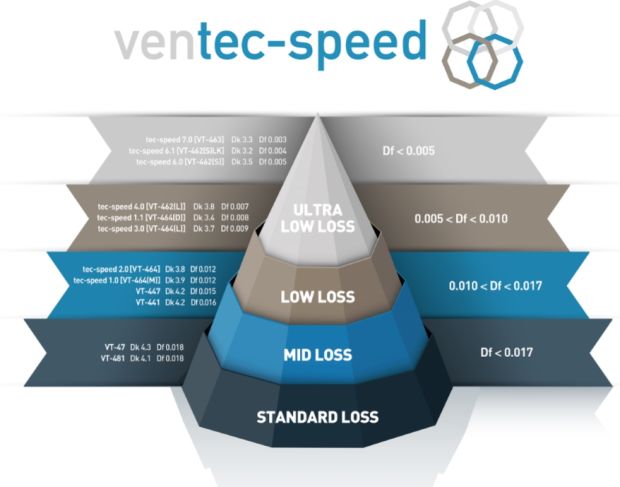
Ventec International Group, a world leader in the production of polyimide & high reliability epoxy laminates and prepregs, will exhibit in Booth 118 at DesignCon 2016 (January 20th to 21st 2016, Santa Clara, CA, USA) where the company will launch a new brand identity, tec-speed, for its high speed/low loss product line. With the launch, Ventec will unveil a new logo, marketing collateral and technical specifications.
The creation of the brand name 'tec-speed' is a move to unite Ventec's high speed/low loss product portfolio and better position the range under a single identity, connecting the products through a clear and cohesive visual presentation.
Martin Cotton, Director OEM Technology, commented: “The tec-speed brand now unites one of the most comprehensive range of products in high speed/low loss PCB material technology. Every tec-speed product provides technological innovation, high performance and quality to customers to perfectly meet their needs.”
Ventec International Group’s COO USA & EUROPE, Mark Goodwin added: “With the growing demand for high reliability and high speed computing & storage applications, and a pipeline of new innovative additions to our range, the timing is right to give our product line a clear identity. More than that, our unique approach to supply chain ownership, with a manufacturing and distribution network that covers the relevant markets globally, ensures fast delivery of quality materials”.
A selection of products will be highlighted at the show, including:
tec-speed 6.1 (Dk 3.2, Df 0.004 RC 50%) - Ultra-Low Loss High Tg material available with all copper styles, including HVLP. Uses Low Dk spread glass to improve Skew and Jitter. Applications include Telecom, Router, Servers etc. Specifically, backplane and daughter card designs where good Signal Integrity is essential. This material has excellent Thermal properties.
tec-speed 4.0 (Dk 3.8, Df 0.007) - Low-Loss High Tg material available with all copper styles, including HVLP. Applications focus on High Frequency & High Speed designs, Automotive and Satellite communication, Navigation, GPS, etc. are typical applications. This material has excellent thermal properties.
tec-speed 1.0 (Dk 3.9, Df 0.012 @ 10GHz RC75%) - Mid-Loss Mid Tg Halogen Free material available with all copper styles. Applications include hand-held products, specifically those that require high frequency high speed materials. This material has excellent thermal properties.
For more information about Ventec’s solutions and the company’s wide variety of products, please visit www.venteclaminates.com or download to the Ventec APP.
About Ventec International
With volume manufacturing facilities and HQ in Suzhou China, Ventec International specializes in advanced copper clad glass reinforced and metal backed substrates for the PCB industry. With distribution locations and quick-turn CCL manufacturing sites in both the US and Europe, Ventec International is a premier supplier to the Global PCB industry. For more information, visit www.venteclaminates.com, www.ventec-usa.com or www.ventec-europe.com.
Share on:


Testimonial
"Advertising in PCB007 Magazine has been a great way to showcase our bare board testers to the right audience. The I-Connect007 team makes the process smooth and professional. We’re proud to be featured in such a trusted publication."
Klaus Koziol - atgSuggested Items
Trouble in Your Tank: Minimizing Small-via Defects for High-reliability PCBs
08/27/2025 | Michael Carano -- Column: Trouble in Your TankTo quote the comedian Stephen Wright, “If at first you don’t succeed, then skydiving is not for you.” That can be the battle cry when you find that only small-diameter vias are exhibiting voids. Why are small holes more prone to voids than larger vias when processed through electroless copper? There are several reasons.
The Government Circuit: Navigating New Trade Headwinds and New Partnerships
08/25/2025 | Chris Mitchell -- Column: The Government CircuitAs global trade winds continue to howl, the electronics manufacturing industry finds itself at a critical juncture. After months of warnings, the U.S. Government has implemented a broad array of tariff increases, with fresh duties hitting copper-based products, semiconductors, and imports from many nations. On the positive side, tentative trade agreements with Europe, China, Japan, and other nations are providing at least some clarity and counterbalance.
How Good Design Enables Sustainable PCBs
08/21/2025 | Gerry Partida, Summit InterconnectSustainability has become a key focus for PCB companies seeking to reduce waste, conserve energy, and optimize resources. While many discussions on sustainability center around materials or energy-efficient processes, PCB design is an often overlooked factor that lies at the heart of manufacturing. Good design practices, especially those based on established IPC standards, play a central role in enabling sustainable PCB production. By ensuring designs are manufacturable and reliable, engineers can significantly reduce the environmental impact of their products.
50% Copper Tariffs, 100% Chip Uncertainty, and a Truce
08/19/2025 | Andy Shaughnessy, I-Connect007If you’re like me, tariffs were not on your radar screen until a few months ago, but now political rhetoric has turned to presidential action. Tariffs are front-page news with major developments coming directly from the Oval Office. These are not typical times. President Donald Trump campaigned on tariff reform, and he’s now busy revamping America’s tariff policy.
Global PCB Connections: Understanding the General Fabrication Process—A Designer’s Hidden Advantage
08/14/2025 | Markus Voeltz -- Column: Global PCB ConnectionsDesigners don’t need to become fabricators, but understanding the basics of PCB fabrication can save you time, money, and frustration. The more you understand what’s happening on the shop floor, the better you’ll be able to prevent downstream issues. As you move into more advanced designs like HDI, flex circuits, stacked vias, and embedded components, this foundational knowledge becomes even more critical. Remember: the fabricator is your partner.