


 It’s Only Common Sense: The Phone Is Still Mightier Than the Keyboard
 The Marketing Minute: Marketing With Layers


Microbots Individually Controlled Using 'Mini Force Fields'
January 13, 2016 | Purdue UniversityEstimated reading time: 3 minutes
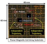
Researchers are using a technology likened to "mini force fields" to independently control individual microrobots operating within groups, an advance aimed at using the tiny machines in areas including manufacturing and medicine.
Until now it was only possible to control groups of microbots to move generally in unison, said David Cappelleri, an assistant professor of mechanical engineering at Purdue University.
"The reason we want independent movement of each robot is so they can do cooperative manipulation tasks," he said. "Think of ants. They can independently move, yet all work together to perform tasks such as lifting and moving things. We want to be able to control them individually so we can have some robots here doing one thing, and some robots there doing something else at the same time."
Findings are detailed in a research paper appearing this month in the journal Micromachines. Postdoctoral research associates Sagar Chowdhury and Wuming Jing, and Cappelleri authored the paper.
The team developed a system for controlling the robots with individual magnetic fields from an array of tiny planar coils.
"The robots are too small to put batteries on them, so they can't have onboard power," Cappelleri said. "You need to use an external way to power them. We use magnetic fields to generate forces on the robots. It's like using mini force fields."
The research is revealing precisely how to control the robots individually.
"We need to know, if a robot is here and it needs to go there, how much force needs to be applied to the robot to get it from point A to point B?" Cappelleri said. "Once you figure out what that force has to be, then we say, what kind of magnetic field strength do we need to generate that force?"
The microbots are magnetic disks that slide across a surface. While the versions studied are around 2 millimeters in diameter – about twice the size of a pinhead - researches aim to create microbots that are around 250 microns in diameter, or roughly the size of a dust mite.
In previously developed systems the microbots were controlled using fewer coils located around the perimeter of the "workspace" containing the tiny machines. However, this "global" field is not fine enough to control individual microrobots independently.
Page 1 of 2
Share on:


Testimonial
"Our marketing partnership with I-Connect007 is already delivering. Just a day after our press release went live, we received a direct inquiry about our updated products!"
Rachael Temple - AlltematedSuggested Items
Episode 6 of Ultra HDI Podcast Series Explores Copper-filled Microvias in Advanced PCB Design and Fabrication
10/15/2025 | I-Connect007I-Connect007 has released Episode 6 of its acclaimed On the Line with... American Standard Circuits: Ultra High Density Interconnect (UHDI) podcast series. In this episode, “Copper Filling of Vias,” host Nolan Johnson once again welcomes John Johnson, Director of Quality and Advanced Technology at American Standard Circuits, for a deep dive into the pros and cons of copper plating microvias—from both the fabricator’s and designer’s perspectives.
Nolan’s Notes: Tariffs, Technologies, and Optimization
10/01/2025 | Nolan Johnson -- Column: Nolan's NotesLast month, SMT007 Magazine spotlighted India, and boy, did we pick a good time to do so. Tariff and trade news involving India was breaking like a storm surge. The U.S. tariffs shifted India from one of the most favorable trade agreements to the least favorable. Electronics continue to be exempt for the time being, but lest you think that we’re free and clear because we manufacture electronics, steel and aluminum are specifically called out at the 50% tariff levels.
MacDermid Alpha & Graphic PLC Lead UK’s First Horizontal Electroless Copper Installation
09/30/2025 | MacDermid Alpha & Graphic PLCMacDermid Alpha Electronics Solutions, a leading supplier of integrated materials and chemistries to the electronics industry, is proud to support Graphic PLC, a Somacis company, with the installation of the first horizontal electroless copper metallization process in the UK.
Electrodeposited Copper Foils Market to Grow by $11.7 Billion Over 2025-2032
09/18/2025 | Globe NewswireThe global electrodeposited copper foils market is poised for dynamic growth, driven by the rising adoption in advanced electronics and renewable energy storage solutions.
MacDermid Alpha Showcases Advanced Interconnect Solutions at PCIM Asia 2025
09/18/2025 | MacDermid Alpha Electronics SolutionsMacDermid Alpha Electronic Solutions, a global leader in materials for power electronics and semiconductor assembly, will showcase its latest interconnect innovations in electronic interconnect materials at PCIM Asia 2025, held from September 24 to 26 at the Shanghai New International Expo Centre, Booth N5-E30