


 The Chemical Connection Onshoring PCB Production—Daunting but Certainly Possible
 It’s Only Common Sense: The Phone Is Still Mightier Than the Keyboard


Time-Based Electrocardiogram (ECG) Readout Chip for Wearable Applications
March 4, 2016 | Holst CentreEstimated reading time: 1 minute
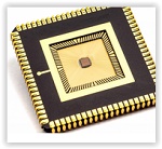
Nanoelectronics research center imec and Holst Centre, an open-innovation initiative set-up by imec and TNO, present a 0.6V ECG readout chip in 40nm technology based on time-domain circuit techniques. The chip maintains consistent beat detection capabilities, even under movement (~40mVpp), paving the way to a low cost, low power multi-sensor Systems-on-Chip (SoCs) solution for wearable medical applications.
There is a clear need for emerging applications in personal healthcare to add more digital signal processing capabilities and memory storage within the system itself. While today's digital ICs and memory ICs benefit from technology scaling in terms of power and area, this has yet to be achieved for analog readout electronics. Current state-of the-art analog circuit techniques don't result in a significantly reduced area in scaled technologies, and due to the accompanied reduced supply voltage (VDD) with scaled technologies, the analog front-end readout chip faces significant challenges in combining a large dynamic range with small size and low power consumption.
The new ECG readout chip is only 0.015mm2 implemented in TSMC 40nm CMOS. It can handle up to 40mVpp AC sigma and up to 300mV DC-electrode offset while consuming only 3.3μW from a 0.6V supply. By acquiring an ECG signal from the noise-stress database, the system does not saturate and is able to maintain a consistent beat detection capability even in presence of vigorous motion (~40mVpp). This was achieved by implementing a time-domain-based readout architecture, which leverages the benefits of technology scaling and it avoids the need for area intensive analog circuitry, such as high-gain amplifiers and passives. The readout chip achieves performance that is comparable with current state-of-the-art implementations at a fraction of the area.
"Our breakthrough readout ECG chip paves the way to low-cost, low-power multi-sensor systems for ambulatory medical applications," stated Nick Van Helleputte, team leader biomedical circuits at imec. "Furthermore, it opens additional innovation paths for beyond 40nm analog front-end design, leveraging the power and area benefits of scaled technology in digital architectures."
Share on:


Testimonial
"The I-Connect007 team is outstanding—kind, responsive, and a true marketing partner. Their design team created fresh, eye-catching ads, and their editorial support polished our content to let our brand shine. Thank you all! "
Sweeney Ng - CEE PCBSuggested Items
KYZEN Brings Reliability to Life at productronica 2025 with ANALYST² Process Control Demos
10/22/2025 | KYZEN'KYZEN, the global leader in innovative environmentally responsible cleaning chemistries, will exhibit at productronica 2025, November 18–21 in Munich, Germany, where the company will put a spotlight on its award-winning KYZEN ANALYST² process control system in Hall A4, Stand 450.
SCHMID Group Secures Major Orders for AI Server PCB Production Equipment
10/22/2025 | SCHMID GroupSCHMID Group, a global equipment maker and solution provider for Printed Circuit Boards (PCB) and IC-Substrate manufacturing – announced the successful acquisition of two significant orders in the fast-growing field of PCB for artificial intelligence (AI) server applications. So called AI-Server-Boards.
SEMICON Japan 2025 to Spotlight Sustainability in AI and Semiconductor Innovation
10/22/2025 | SEMISEMICON Japan 2025, the largest gathering of leaders from the microelectronics manufacturing supply chain in Japan, will bring together more than 1,200 exhibitors showcasing semiconductor solutions from December 17-19 at Tokyo Big Sight.
Circus SE Set for High-Volume Market Entry in the Defense Sector
10/17/2025 | BUSINESS WIRECircus SE a global technology leader in AI robotics for autonomous nutrition systems and troop supply, is expanding its global production network as part of its high-volume market entry into the defense sector.
China Expands Rare Earth Export Restrictions, Tightening Grip on Global Supply Chains
10/16/2025 | I-Connect007 Editorial TeamChina sharply expanded its rare earth export restrictions on Oct. 9, adding additional elements and refining technologies to its control list while imposing stricter rules on foreign users in the defense and semiconductor industries.