


 Dan’s Biz Bookshelf: ‘Do/Start'
 Facing the Future: The Role of 5G and Beyond in Shaping PCB Demand
 It’s Only Common Sense: Stop Pitching, Start Listening


Enabling Extreme New Designs for Optics and Imagers
August 22, 2016 | DARPAEstimated reading time: 2 minutes
Developers of imaging systems have long been beholden to certain rules of optics designs so well established and seemingly immutable as to be treated as virtual “laws” of physics. One widely considered pillar of optical design, for example, is that imaging systems must be built from a series of complex and precisely manufactured optical elements arranged linearly. The result of such assumptions is that certain high-performance imagery devices inevitably end up being large and heavy, composed of dozens or more optical elements. DARPA’s EXTREME Optics and Imaging (EXTREME) program aims to break from that well-worn paradigm by introducing engineered optical materials (EnMats) and associated design tools for creating innovative optical systems with improved performance, new functionality, and drastically reduced size and weight.
A special notice was issued today announcing the EXTREME Proposers Day on September 1, 2016, via webcast to familiarize potential proposers with the goals of the program. A Broad Agency Announcement solicitation is also expected to be posted on DARPA’s FedBizOpps page in the near future.
“We’ve seen significant technical advances in recent years in the communities of optical system design, materials science and fabrication, and multiscale modeling and optimization,” said Predrag Milojkovic, DARPA program manager. “EXTREME seeks to capitalize on this momentum by uniting these separate communities to revolutionize optics and imaging as we know it.”
To achieve its goal, EXTREME is focused on developing new EnMats—both two-dimensional metasurfaces as well as 3-D volumetric optics and holograms—that manipulate light in ways beyond classical rules of reflection and refraction. EXTREME also will address multiscale modelling to enable design and optimization of EnMats across vastly different scales, from nanometer to centimeter, for example.
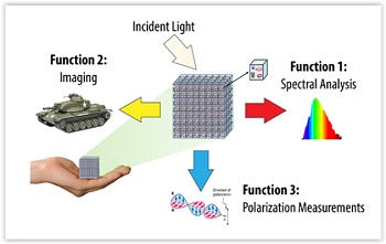
The program aims to demonstrate an optical system with engineered surfaces where control of light propagation is decoupled from a specific geometric shape and can be tuned. EXTREME also seeks to demonstrate a volumetric optical element the size of a sugar cube or larger that can perform a multitude of functions simultaneously in visual and infrared (IR) bands, such as imaging, spectrum analysis, and polarization measurements, among others.
If successful, EXTREME could introduce a new era in optics and imagers for national defense. EXTREME optical components would be lighter and smaller, enabling miniaturization of imaging systems for intelligence, surveillance, and reconnaissance (ISR) applications. The multifunctional nature of these devices could offer improvements in a wide variety of imaging systems by reducing size and weight without compromising performance for systems as diverse as night vision goggles, hyperspectral imagers, and IR search and track systems.
DARPA anticipates that reaching the objectives of the EXTREME program will require formation of cross-cutting teams bringing together expertise from disparate communities and fields, including but not limited to engineered material design and fabrication, multiscale modeling/simulation/optimization, and optical system design. Details on the upcoming Proposers Day are available here.
Share on:


Suggested Items
Canadian Circuits Inc. Unveils Rapid Prototype PCB Assembly Service to Accelerate Innovation
05/14/2025 | Canadian Circuits, Inc.Canadian Circuits Inc. (CCI), a leading provider of high-quality, made-in-Canada, Printed Circuit Board (PCB) solutions, is proud to announce the launch of its Prototype PCB Assembly (PCBA) service. This new offering enhances CCI’s commitment to empowering engineers and OEMs by accelerating the journey from concept to product launch with precision and efficiency in electronics manufacturing.
New Episode of NCAB Podcast Series Explores Cutting-edge Thermal Management Solutions
05/14/2025 | I-Connect007In this episode we continue the conversation with NCAB Field Application Engineer Ryan Miller as we dive into practical design and manufacturing techniques for controlling thermal effects. Topics include via farms, insulated metal substrates, coin technology, and copper pedestals—solutions that help meet today's high-performance demands.
American Standard Circuits to Exhibit and Speak at SMTA Oregon Expo
05/14/2025 | American Standard CircuitsAnaya Vardya, President, and CEO of American Standard Sunstone Circuits has announced that his company will be exhibiting SMTA Oregon Expo & Tech Forum to be held on May 20 at the Wingspan Events and Conference Center in Hillsboro, Oregon.
indie Semiconductor Reports Q1 2025 Results
05/13/2025 | BUSINESS WIREindie Semiconductor, Inc., an automotive solutions innovator, today announced first quarter results for the period ended March 31, 2025. Q1 revenue was up 3.3 percent year-over-year to $54.1 million with Non-GAAP gross margin of 49.5 percent. On a GAAP basis, first quarter 2025 operating loss was $38.9 million compared to $49.6 million a year ago.
Elementary, Mr. Watson: Design Data Packages—Circle of Concern or Circle of Influence?
05/14/2025 | John Watson -- Column: Elementary, Mr. WatsonI've often been asked, "Can you have a perfect PCB design?" At first blush, it seems like the answer should be yes. After all, if you follow all the rules, double-check your work, and use the right tools, it should be perfect. Right?