


 Dan's Biz Bookshelf: 'Getting Naked: A Business Fable'
 The Chemical Connection: Common Misconceptions in Wet Processing
 It’s Only Common Sense: Selling to Engineers


Researchers Control 'shear-band' Defects in Manufacturing Processes
September 22, 2016 | Purdue UniversityEstimated reading time: 4 minutes
An international team of researchers has invented a method to control the formation of defects called "shear bands" in metals manufacturing processes and discovered microscopic details of how the defects are created.
Shear banding occurs often in high-speed machining of structural metals. It has been a long-standing problem in manufacturing processes because it hinders production of good quality surfaces while machining advanced metal alloys like titanium, nickel and high-temperature aerospace materials, and in the production of metal sheets and foils, according to Srinivasan Chandrasekar, a Purdue University professor of industrial engineering and Kevin P. Trumble, a professor of materials engineering.
"This new work, based on a fundamental understanding of how shear bands form, is an important advance for manufacturing and metals processing," said Chandrasekar, director of Purdue's Center for Materials Processing and Tribology.
The research has revealed that the shear bands form in two phases, said Purdue postdoctoral research associate Koushik Viswanathan.
First, a "weak interface" is created as the metal is being cut, and then the metal shears at this interface, producing a saw-tooth pattern.
The formation of "shear bands" has been a long-standing problem in metals manufacturing processes. The phenomenon is seen in the electron microscope image at left as a wavy saw-toothed structure in a peeled strip of titanium. At right top, the researchers traced a "micromarker" across a shear band, highlighted in yellow. At bottom right an electron back scatter image reveals the band as a severely deformed, dark featureless region about four micrometers thick.
"More importantly, we have learned how to suppress the formation of shear bands using a simple method," said lead author Dinakar Sagapuram, a former Purdue postdoctoral research associate who recently joined Texas A&M University as an assistant professor.
Findings are detailed in a paper published online in August in the Proceedings of the Royal Society A, and featured on the cover of the September print edition of the journal.
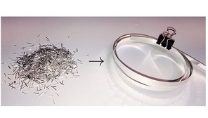
Chandraekar sherbands2 An international team of researchers has invented a method to control the formation of defects called "shear bands" in metals manufacturing processes. At left, the defects create chips of needle-shaped particles. At right, the new method eliminates the shear banding, resulting in a long continuous strip. (Purdue University image/Center for Materials Processing and Tribology) Download image
The phenomenon of shear-band formation exists in many settings, from the nearly atomic scale in "metallic glasses," to the millimeter scale in machined metals and to kilometer-size defects seen in rocks that undergo sliding in the earth's crust.
The "displacement profiles" of shear bands resemble those created in liquids flowing past an interface. Because of this similarity, the researchers applied mathematical equations customarily used to analyze viscous fluid flow to analyze the formation of the shear bands. The fluid-like behavior is mysterious because it is unclear whether the metals being processed heat up enough to actually become liquid.
"The temperatures generated in these shear bands have been estimated from a few hundred Celsius to a few thousand Celsius, so this is really an unknown," Viswanathan said.
The first phase of the band formation occurs within just a few microseconds.
"The second phase is where the metal slides along a thin weak interface," Sagapuram said. "This phase is somewhat more gradual and surprisingly exhibits a viscous-like behavior."
The suppression method works by adding a wedge-shaped die opposite the cutting tool, so that the chip from the metal being machined is channeled between the two. The additional tool constrains the metal to deform more uniformly and eliminates the viscous sliding phase. Because of its simplicity, the method is practical for use in industry.
"You can think of it as the tool consisting of two parts, one doing the cutting and other doing the constraining," said Chandrasekar, also a professor of materials engineering.
The paper was authored by Sagapuram, Viswanathan, Chandrasekar and Trumble; Anirban Mahato, an assistant professor at the Indian Institute of Technology, Patna; Narayan K. Sundaram, an assistant professor at the Indian Institute of Science; and Rachid M'Saoubi, a research manager at Seco Tools Ltd. in the United Kingdom.
The researchers studied the deformation by taking images of marks etched into the metal beforehand. As the metal is processed, the groove-like "micromarkers" reveal the large and serrated deformations.
"The markers basically tell you if the deformation is homogeneous or not, and also how much deformation the material has locally undergone near the shear band defects," Trumble said.
The shear bands form parallel, intensely deformed striations and may cause the metal to break into fragments small enough to produce a powder-like pile of chip shavings. Metals like titanium and magnesium, which have a hexagonal close-packed crystal structure, are particularly prone to the shear band formation. However, the bands can form also in other metals that do not have this crystal structure, including brass, copper, steels and superalloys.
Several patent applications related to the research were filed through the Purdue Research Foundation's Office of Technology Commercialization.
The work was funded by the U.S. Department of Energy, U.S. Army Research Office and National Science Foundation.
Share on:


Suggested Items
Elephantech: For a Greener Tomorrow
04/16/2025 | Marcy LaRont, PCB007 MagazineNobuhiko Okamoto is the global sales and marketing manager for Elephantech Inc., a Japanese startup with a vision to make electronics more sustainable. The company is developing a metal inkjet technology that can print directly on the substrate and then give it a copper thickness by plating. In this interview, he discusses this novel technology's environmental advantages, as well as its potential benefits for the PCB manufacturing and semiconductor packaging segments.
Trouble in Your Tank: Organic Addition Agents in Electrolytic Copper Plating
04/15/2025 | Michael Carano -- Column: Trouble in Your TankThere are numerous factors at play in the science of electroplating or, as most often called, electrolytic plating. One critical element is the use of organic addition agents and their role in copper plating. The function and use of these chemical compounds will be explored in more detail.
IDTechEx Highlights Recyclable Materials for PCBs
04/10/2025 | IDTechExConventional printed circuit board (PCB) manufacturing is wasteful, harmful to the environment and energy intensive. This can be mitigated by the implementation of new recyclable materials and technologies, which have the potential to revolutionize electronics manufacturing.
Connect the Dots: Stop Killing Your Yield—The Hidden Cost of Design Oversights
04/03/2025 | Matt Stevenson -- Column: Connect the DotsI’ve been in this industry long enough to recognize red flags in PCB designs. When designers send over PCBs that look great on the computer screen but have hidden flaws, it can lead to manufacturing problems. I have seen this happen too often: manufacturing delays, yield losses, and designers asking, “Why didn’t anyone tell me sooner?” Here’s the thing: Minor design improvements can greatly impact manufacturing yield, and design oversights can lead to expensive bottlenecks. Here’s how to find the hidden flaws in a design and avoid disaster.
Real Time with... IPC APEX EXPO 2025: Tariffs and Supply Chains in U.S. Electronics Manufacturing
04/01/2025 | Real Time with...IPC APEX EXPOChris Mitchell, VP of Global Government Relations for IPC, discusses IPC's concerns about tariffs on copper and their impact on U.S. electronics manufacturing. He emphasizes the complexity of supply chains and the need for policymakers to understand their effects.