


 The Marketing Minute: Cracking the Code of Technical Marketing
 Trouble in Your Tank: Implementing Direct Metallization in Advanced Substrate Packaging


A Conscious Coupling of Magnetic and Electric Materials
September 23, 2016 | LBLEstimated reading time: 6 minutes
Scientists have successfully paired ferroelectric and ferrimagnetic materials so that their alignment can be controlled with a small electric field at near room temperatures, an achievement that could open doors to ultra low-power microprocessors, storage devices and next-generation electronics.
Scientists engineered a new magnetic ferroelectric at the atomic-scale. A false-colored electron microscopy image shows alternating lutetium (yellow) and iron (blue) atomic planes. An extra plane of iron atoms was inserted every ten repeats, substantially changing the magnetic properties. (Credit: Emily Ryan and Megan Holtz/Cornell)
The work, co-led by researchers at the Department of Energy’s Lawrence Berkeley National Laboratory (Berkeley Lab) and Cornell University, is described in a study to be published Sept. 22 in the journal Nature.
The researchers engineered thin, atomically precise films of hexagonal lutetium iron oxide (LuFeO3), a material known to be a robust ferroelectric, but not strongly magnetic. Lutetium iron oxide consists of alternating single monolayers of lutetium oxide and single monolayers of iron oxide, and differs from a strong ferrimagnetic oxide that consists of alternating monolayers of lutetium oxide with double monolayers of iron oxide (LuFe2O4).
The researchers found that by carefully adding one extra monolayer of iron oxide to every 10 atomic repeats of the single-single monolayer pattern, they could dramatically change the material’s properties and produce a strongly ferrimagnetic layer near room temperature. They then tested the new material to show that the ferrimagnetic atoms followed the alignment of their ferroelectric neighbors when switched by an electric field.
They did this at temperatures ranging from 200-300 kelvins (minus 100 to 80 degrees Fahrenheit), relatively balmy compared with other such multiferroics that typically work at much lower temperatures.
“Developing materials that can work at room temperature makes them viable candidates for today’s electronics,” said study co-lead author Julia Mundy, a University of California Presidential Postdoctoral Fellow and an affiliate at Berkeley Lab. “The multiferroic we created takes us a major step toward that goal.”
Researchers have increasingly sought alternatives to semiconductor-based electronics over the past decade as the increases in speed and density of microprocessors come at the expense of greater demands on electricity and hotter circuits.
“If you look at this in a broad sense, about 5 percent of our total global energy consumption is spent on electronics,” said co-senior author Ramamoorthy Ramesh, Berkeley Lab’s Associate Laboratory Director for Energy Technologies and a UC Berkeley professor of materials science and engineering and of physics. “It’s the fastest growing consumer of energy worldwide. The Internet of Things is leading to the installation of electronic devices everywhere. The world’s energy consumed by microelectronics is projected to be 40-50 percent by 2030 if we continue at the current pace and if there are no major advances in the field that lead to lower energy consumption.”
A major path to reducing energy consumption involves ferroic materials. Key advantages of ferroelectrics include their reversible polarization in response to low-power electric fields, and their ability to hold their polarized state without the need for continuous power. Common examples of ferroelectric materials include transit cards and, more recently, memory chips.
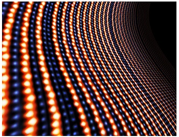
The researchers use electric fields to create concentric boxes of "up" and "down" ferroelectric polarization (shown left in red and turquoise) in the lutetium ferrite film. They then use photo emission electron microscopy at the Advanced Light Source to read out the magnetic structure from this region, demonstrating that the magnetism directly tracks the ferroelectric structure even though no magnetic fields were applied. The scale bar is 5 microns. (Credit: James Clarkson, Alan Farhan, and Andreas Scholl/Berkeley Lab)
Ferromagnets and ferrimagnets have similar features, responding to magnetic fields, and are used in hard drives and sensors.
Pairing ferroelectric and ferrimagnetic materials into one multiferroic film would capture the advantages of both systems, enabling a wider range of memory applications with minimal power requirements. It has been an uneasy marriage, however, because the forces needed to align one type of material fail to work for the other. Polarizing the ferroelectric material would have no effect on the ferrimagnetic one.
Mundy began to tackle this challenge of creating a viable multiferroic while she was a Cornell University graduate student in the lab of Darrell Schlom, a professor of materials science and engineering and a leading expert in molecular-beam epitaxy. The ultra-precise technique – something Schlom likens to atomic spray painting – allowed the researchers to design and assemble the two different materials atom by atom, layer after layer. They intentionally seated a lutetium iron oxide with alternating iron oxide double layers (LuFe2O4) next to lutetium iron oxide with alternating iron oxide single layers (LuFeO3), and that positioning made all the difference in nudging the ferrimagnetic atoms to move in conjunction with the ferroelectric ones.
To show that this coupling was working at the atomic level, the researchers took the multiferroic film created at Cornell to Berkeley Lab’s Advanced Light Source (ALS). There, they had the equipment and expertise to test the material and capture images of the result using photoemission electron microscopy.
Working with staff scientists Andreas Scholl and Elke Arenholz at the ALS, they used a 5-volt probe from an atomic force microscope to switch the polarization of the ferroelectric material up and down, creating a geometric pattern of concentric squares. They then showed that the ferrimagnetic regions within the layered sample displayed the same pattern, even though no magnetic field was used. The direction was controlled by the electric field generated by the probe.
“It was when our collaborators at Berkeley Lab demonstrated electrical control of magnetism in the material that we made that things got super exciting!” said Schlom at Cornell. “Room-temperature multiferroics are rare. Including our new material, a total of four are known, but only one room-temperature multiferroic was known in which magnetism could be controlled electrically. Our work shows that an entirely different mechanism is active in this new material, giving us hope for even better — higher temperature and stronger — manifestations for the future.”
The researchers next plan to explore strategies for lowering the voltage threshold for influencing the direction of polarization. This includes experimenting with different substrates for building new materials.
“We want to show that this works at half a volt as well as at 5 volts,” said Ramesh. “We also want to make a working device with the multiferroic.”
Hena Das, a visiting scientist at Berkeley Lab and associate specialist at UC Berkeley, is another co-author on the study. Das started the work as a postdoctoral researcher at Cornell University and is the lead theorist on the study.
The Department of Energy’s Office of Science helped support this work. The ALS is a DOE Office of Science User Facility.
About Lawrence Berkeley National Laboratory
Lawrence Berkeley National Laboratory addresses the world’s most urgent scientific challenges by advancing sustainable energy, protecting human health, creating new materials, and revealing the origin and fate of the universe. Founded in 1931, Berkeley Lab’s scientific expertise has been recognized with 13 Nobel prizes. The University of California manages Berkeley Lab for the U.S. Department of Energy’s Office of Science.
About DOE
DOE’s Office of Science is the single largest supporter of basic research in the physical sciences in the United States, and is working to address some of the most pressing challenges of our time.
Share on:


Testimonial
"In a year when every marketing dollar mattered, I chose to keep I-Connect007 in our 2025 plan. Their commitment to high-quality, insightful content aligns with Koh Young’s values and helps readers navigate a changing industry. "
Brent Fischthal - Koh YoungSuggested Items
Curing and Verification in PCB Shadow Areas
09/17/2025 | Doug Katze, DymaxDesign engineers know a simple truth that often complicates electronics manufacturing: Light doesn’t go around corners. In densely populated PCBs, adhesives and coatings often fail to fully cure in shadowed regions created by tall ICs, connectors, relays, and tight housings.
Marcy’s Musings: Advancing the Advanced Materials Discussion
09/17/2025 | Marcy LaRont -- Column: Marcy's MusingsAs the industry’s most trusted global source of original content about the electronics supply chain, we continually ask you about your concerns, what you care about, and what you most want to learn about. Your responses are insightful and valuable. Thank you for caring enough to provide useful feedback and engage in dialogue.
September 2025 PCB007 Magazine: The Future of Advanced Materials
09/16/2025 | I-Connect007 Editorial TeamMoore’s Law is no more, and the advanced material solutions being developed to grapple with this reality are surprising, stunning, and perhaps a bit daunting. Buckle up for a dive into advanced materials and a glimpse into the next chapters of electronics manufacturing.
I-Connect007 Launches Advanced Electronics Packaging Digest
09/15/2025 | I-Connect007I-Connect007 is pleased to announce the launch of Advanced Electronics Packaging Digest (AEPD), a new monthly digital newsletter dedicated to one of the most critical and rapidly evolving areas of electronics manufacturing: advanced packaging at the interconnect level.
Panasonic Industry will Double the Production Capacity of MEGTRON Multi-layer Circuit Board Materials Over the Next Five Years
09/15/2025 | Panasonic Industry Co., Ltd.Panasonic Industry Co., Ltd., a Panasonic Group company, announced plans for a major expansion of its global production capacity for MEGTRON multi-layer circuit board materials today. The company plans to double its production over the next five years to meet growing demand in the AI server and ICT infrastructure markets.