


 The Marketing Minute: Cracking the Code of Technical Marketing
 Trouble in Your Tank: Implementing Direct Metallization in Advanced Substrate Packaging


Mysterious Quantum Properties in Material Point to New Applications in Electronics
September 26, 2016 | Lawrence Berkeley National LaboratoryEstimated reading time: 5 minutes
Researchers have created an exotic 3-D racetrack for electrons in ultrathin slices of a nanomaterial they fabricated at the Department of Energy’s Lawrence Berkeley National Laboratory (Berkeley Lab).
The international team of scientists from Berkeley Lab, UC Berkeley, and Germany observed, for the first time, a unique behavior in which electrons rotate around one surface, then through the bulk of the material to its opposite surface and back.
The possibility of developing so-called “topological matter” that can carry electrical current on its surface without loss at room temperature has attracted significant interest in the research community. The ultimate goal is to approach the lossless conduction of another class of materials, known as superconductors, but without the need for the extreme, freezing temperatures that superconductors require.
“Microchips lose so much energy through heat dissipation that it’s a limiting factor,” said James Analytis, a staff scientist at Berkeley Lab and assistant professor of physics at UC Berkeley who led the study, published in Nature. “The smaller they become, the more they heat up.”
The studied material, an inorganic semimetal called cadmium arsenide (Cd3As2), exhibits quantum properties—which are not explained by the classical laws of physics—that offer a new approach to reducing waste energy in microchips. In 2014, scientists discovered that cadmium arsenide shares some electronic properties with graphene, a single-atom-thick material also eyed for next-generation computer components, but in a 3-D form.
“What’s exciting about these phenomena is that, in theory, they are not affected by temperature, and the fact they exist in three dimensions possibly makes fabrication of new devices easier,” Analytis said.
The cadmium arsenide samples displayed a quantum property known as “chirality” that couples an electron’s fundamental property of spin to its momentum, essentially giving it left- or right-handed traits. The experiment provided a first step toward the goal of using chirality for transporting charge and energy through a material without loss.
In the experiment, researchers manufactured and studied how electric current travels in slices of a cadmium arsenic crystal just 150 nanometers thick, or about 600 times smaller than the width of a human hair, when subjected to a high magnetic field.
The crystal samples were crafted at Berkeley Lab’s Molecular Foundry, which has a focus in building and studying nanoscale materials, and their 3-D structure was detailed using X-rays at Berkeley Lab’s Advanced Light Source.
Many mysteries remain about the exotic properties of the studied material, and as a next step researchers are seeking other fabrication techniques to build a similar material with built-in magnetic properties, so no external magnetic field is required.
“This isn’t the right material for an application, but it tells us we’re on the right track,” Analytis said.
If researchers are successful in their modifications, such a material could conceivably be used for constructing interconnects between multiple computer chips, for example, for next-generation computers that rely on an electron’s spin to process data (known as “spintronics”), and for building thermoelectric devices that convert waste heat to electric current.
It wasn’t clear at first whether the research team would even be able to manufacture a pure enough sample at the tiny scale required to carry out the experiment, Analytis said.
“We wanted to measure the surface states of electrons in the material. But this 3-D material also conducts electricity in the bulk—it’s central region—as well as at the surface,” he said. As a result, when you measure the electric current, the signal is swamped by what is going on in the bulk so you never see the surface contribution.”
So they shrunk the sample from millionths of a meter to the nanoscale to give them more surface area and ensure that the surface signal would be the dominant one in an experiment.
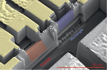
This image, produced by a scanning electron microscope, shows three sheets of a crystal material called cadmium arsenide. The finely polished rectangular sheets (purple) were sliced from the same crystal in varying thicknesses. They measure about 4 microns (thousandths of a millimeter) tall by 10 microns wide.
Page 1 of 2
Share on:


Testimonial
"In a year when every marketing dollar mattered, I chose to keep I-Connect007 in our 2025 plan. Their commitment to high-quality, insightful content aligns with Koh Young’s values and helps readers navigate a changing industry. "
Brent Fischthal - Koh YoungSuggested Items
Curing and Verification in PCB Shadow Areas
09/17/2025 | Doug Katze, DymaxDesign engineers know a simple truth that often complicates electronics manufacturing: Light doesn’t go around corners. In densely populated PCBs, adhesives and coatings often fail to fully cure in shadowed regions created by tall ICs, connectors, relays, and tight housings.
Marcy’s Musings: Advancing the Advanced Materials Discussion
09/17/2025 | Marcy LaRont -- Column: Marcy's MusingsAs the industry’s most trusted global source of original content about the electronics supply chain, we continually ask you about your concerns, what you care about, and what you most want to learn about. Your responses are insightful and valuable. Thank you for caring enough to provide useful feedback and engage in dialogue.
September 2025 PCB007 Magazine: The Future of Advanced Materials
09/16/2025 | I-Connect007 Editorial TeamMoore’s Law is no more, and the advanced material solutions being developed to grapple with this reality are surprising, stunning, and perhaps a bit daunting. Buckle up for a dive into advanced materials and a glimpse into the next chapters of electronics manufacturing.
I-Connect007 Launches Advanced Electronics Packaging Digest
09/15/2025 | I-Connect007I-Connect007 is pleased to announce the launch of Advanced Electronics Packaging Digest (AEPD), a new monthly digital newsletter dedicated to one of the most critical and rapidly evolving areas of electronics manufacturing: advanced packaging at the interconnect level.
Panasonic Industry will Double the Production Capacity of MEGTRON Multi-layer Circuit Board Materials Over the Next Five Years
09/15/2025 | Panasonic Industry Co., Ltd.Panasonic Industry Co., Ltd., a Panasonic Group company, announced plans for a major expansion of its global production capacity for MEGTRON multi-layer circuit board materials today. The company plans to double its production over the next five years to meet growing demand in the AI server and ICT infrastructure markets.