


 The Marketing Minute: Cracking the Code of Technical Marketing
 Trouble in Your Tank: Implementing Direct Metallization in Advanced Substrate Packaging


Record for Perovskite/CIGS Tandem Solar Module
September 27, 2016 | KITEstimated reading time: 2 minutes
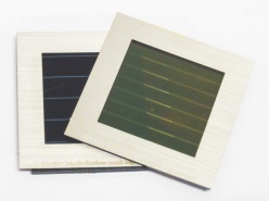
Thin-film technologies can dramatically reduce the cost of next-generation solar modules. Whereas their production cost is low, it is in particular the combination of complementary absorber materials in a tandem solar module that increases the power conversion efficiency. At the PSCO international conference in Genova, researchers from KIT, ZSW, and the Belgian research institute imec present a perovskite/CIGS tandem thin-film solar module that achieves 17.8 percent in efficiency, surpassing for the first time the efficiency of separate perovskite and CIGS solar modules.
“Our prototype demonstrates that scalable perovskite/CIGS solar modules can drastically surpass the efficiency of a separate solar module made of these materials,” emphasizes Dr. Ulrich W. Paetzold of KIT. His newly established young investigators group at KIT’s Institute of Microstructure Technology and Institute of Light Technology investigates and optimizes light trapping and energy efficiency in these tandem solar modules.
Professor Michael Powalla, head of the Thin-film Photovoltaics Division at KIT as well as member of the board and head of the Photovoltaics Division at ZSW, points out: “The novel stacked module is an elegant way of making optimum use of a large part of the solar spectrum by combining the advantages of two highly innovative thin-film technologies.” Whereas the semitransparent upper perovskite solar module efficiently absorbs the high-energy portion of the solar spectrum, the lower CIGS (Copper Indium Gallium Selenide) layer converts the infrared parts. In total, the prototype achieves an energy conversion efficiency of 17.8 percent. For comparison, the current world record for perovskite modules on this scale is at 15.3 percent, and the reference CIGS solar module has an efficiency of 15.7 percent.
Besides, the stacked module implements a fully scalable device concept that matches industrial needs. Both, the perovskite top module and the CIGS bottom module feature an aperture area of 3.67 square centimeter and a monolithic interconnection scheme, using 4 and 7 module cell stripes respectively. The area losses are less than 8 percent for both technologies and the interconnection can be laser-processed, allowing industrial scaling to stacked modules of several square meters. All previous reports on this technology have been limited to very small scale solar cells. The presented achievement takes the technology to large area and scalable solar module architecture which show remarkable power conversion efficiencies.
Tom Aernouts, team leader head of thin-film PV research at imec commented: “This result was made possible by combining the complementary world-leading expertise of the three partners in a very fruitful collaboration.” Whereas the Belgian research institute imec is a leader in the manufacture of semitransparent perovskite solar modules, ZSW is a pioneer in the development and scaling of CIGS-based solar cells and modules and holds the efficiency world record of 22.6 percent for CIGS thin-film solar cells which are the basic elements for interconnected solar modules. The Helmholtz Young Investigators Group at KIT, headed by Dr. Ulrich W. Paetzold, studies the optics in these components and develops new nanophotonic materials for improved light harvesting.
Share on:


Testimonial
"The I-Connect007 team is outstanding—kind, responsive, and a true marketing partner. Their design team created fresh, eye-catching ads, and their editorial support polished our content to let our brand shine. Thank you all! "
Sweeney Ng - CEE PCBSuggested Items
Trouble in Your Tank: Implementing Direct Metallization in Advanced Substrate Packaging
09/15/2025 | Michael Carano -- Column: Trouble in Your TankDirect metallization systems based on conductive graphite are gaining popularity throughout the world. The environmental and productivity gains achievable with this process are outstanding. Direct metallization reduces the costs of compliance, waste treatment, and legal issues related to chemical exposure. A graphite-based direct plate system has been devised to address these needs.
Closing the Loop on PCB Etching Waste
09/09/2025 | Shawn Stone, IECAs the PCB industry continues its push toward greener, more cost-efficient operations, Sigma Engineering’s Mecer System offers a comprehensive solution to two of the industry’s most persistent pain points: etchant consumption and rinse water waste. Designed as a modular, fully automated platform, the Mecer System regenerates spent copper etchants—both alkaline and acidic—and simultaneously recycles rinse water, transforming a traditionally linear chemical process into a closed-loop system.
Driving Innovation: Depth Routing Processes—Achieving Unparalleled Precision in Complex PCBs
09/08/2025 | Kurt Palmer -- Column: Driving InnovationIn PCB manufacturing, the demand for increasingly complex and miniaturized designs continually pushes the boundaries of traditional fabrication methods, including depth routing. Success in these applications demands not only on robust machinery but also sophisticated control functions. PCB manufacturers rely on advanced machine features and process methodologies to meet their precise depth routing goals. Here, I’ll explore some crucial functions that empower manufacturers to master complex depth routing challenges.
Trouble in Your Tank: Minimizing Small-via Defects for High-reliability PCBs
08/27/2025 | Michael Carano -- Column: Trouble in Your TankTo quote the comedian Stephen Wright, “If at first you don’t succeed, then skydiving is not for you.” That can be the battle cry when you find that only small-diameter vias are exhibiting voids. Why are small holes more prone to voids than larger vias when processed through electroless copper? There are several reasons.
The Government Circuit: Navigating New Trade Headwinds and New Partnerships
08/25/2025 | Chris Mitchell -- Column: The Government CircuitAs global trade winds continue to howl, the electronics manufacturing industry finds itself at a critical juncture. After months of warnings, the U.S. Government has implemented a broad array of tariff increases, with fresh duties hitting copper-based products, semiconductors, and imports from many nations. On the positive side, tentative trade agreements with Europe, China, Japan, and other nations are providing at least some clarity and counterbalance.