


 The Marketing Minute: Cracking the Code of Technical Marketing
 Trouble in Your Tank: Implementing Direct Metallization in Advanced Substrate Packaging


Lowering the Heat Makes New Materials Possible While Saving Energy
September 29, 2016 | Pennsylvania State UniversityEstimated reading time: 3 minutes
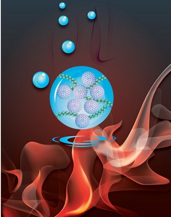
A new technology developed by Penn State researchers, called cold sintering process (CSP), opens a window on the ability to combine incompatible materials, such as ceramics and plastics, into new, useful compound materials, and to lower the energy cost of many types of manufacturing.
Ceramics is the oldest known man-made material, dating back tens of thousands of years. Throughout that time nearly all ceramics were made by heating to high temperatures, either by firing in kilns or sintering ceramic powders in furnaces, both of which require large amounts of energy.
"In this day and age, when we have to be incredibly conscious of the carbon dioxide budget, the energy budget, rethinking many of our manufacturing processes, including ceramics, becomes absolutely vital," said Clive Randall, professor of materials science and engineering at Penn State who developed the process with his team. "Not only is this a low temperature process (room temperature up to 200 degrees Celsius), but we are also densifying some materials to over 95 percent of their theoretical density in 15 minutes. We can now make a ceramic faster than you can bake a pizza, and at lower temperatures."
In a recent article in Advanced Functional Materials, Randall and his coauthors describe the co-sintering of ceramic and thermoplastic polymer composites using CSP. Three types of polymer were selected to complement the properties of three types of ceramics -- a microwave dielectric, an electrolyte and a semiconductor -- in order to highlight the diversity of applicable materials. These composite materials demonstrate new possibilities for dielectric property design, and both ionic and electronic electrical conductivity design. These composites can be sintered to high density at 120 degrees Celsius in 15 to 60 minutes.
According to the researchers, the process involves wetting ceramic powder with a few drops of water or acid solution. The solid surfaces of the particles decompose and partially dissolve in the water to produce a liquid phase at particle-to-particle interfaces. Adding temperature and pressure causes the water to flow and the solid particles to rearrange in an initial densification process. Then in a second process, clusters of atoms or ions move away from where the particles are in contact, aiding diffusion, which then minimizes surface free energy, allowing the particles to pack tightly together. The key is knowing the exact combination of moisture, pressure, heat and time required to capture the reaction rates so the material fully crystallizes and gets to very high density.
"I see cold sintering process as a continuum of different challenges," Randall said. "In some systems, it's so easy you don't need pressure. In others you do. In some you need to use nanoparticles. In others, you can get away with a mixture of nanoparticles and larger particles. It really all depends on the systems and chemistries you are talking about."
The Penn State team has begun building a library of the precise techniques required to use CSP on various materials systems, with 50 processes verified to-date. These include ceramic-ceramic composites, ceramic-nanoparticle composites, ceramic-metals, as well as the ceramic-polymers discussed in this paper.
Other areas that are now open to exploration by CSP include architectural materials, such as ceramic bricks, thermal insulation, biomedical implants and many types of electronic components.
"My hope is that a lot of the manufacturing processes that already exist will be able to use this process, and we can learn from polymer manufacturing practices," Randall concluded.
Co-authors on "Cold Sintering Process of Composites: Bridging the Processing Temperature Gap of Ceramics and Polymer Materials" were postdoctoral scholars Jing Guo and Hanzheng Guo, Ph.D. candidate Seth Berbano, research and development engineer Amanda Baker, and Michael Lanagan, professor of engineering science and mechanics, all part of Penn State's Materials Research Institute.
The National Science Foundation as part of the Center for Dielectrics and Piezoelectrics and the NSF-ERC ASSIST program, the 3M Science and Technology Fellowship and the Department of Energy GATE Fellowship supported this work.
Share on:


Testimonial
"Advertising in PCB007 Magazine has been a great way to showcase our bare board testers to the right audience. The I-Connect007 team makes the process smooth and professional. We’re proud to be featured in such a trusted publication."
Klaus Koziol - atgSuggested Items
Curing and Verification in PCB Shadow Areas
09/17/2025 | Doug Katze, DymaxDesign engineers know a simple truth that often complicates electronics manufacturing: Light doesn’t go around corners. In densely populated PCBs, adhesives and coatings often fail to fully cure in shadowed regions created by tall ICs, connectors, relays, and tight housings.
Marcy’s Musings: Advancing the Advanced Materials Discussion
09/17/2025 | Marcy LaRont -- Column: Marcy's MusingsAs the industry’s most trusted global source of original content about the electronics supply chain, we continually ask you about your concerns, what you care about, and what you most want to learn about. Your responses are insightful and valuable. Thank you for caring enough to provide useful feedback and engage in dialogue.
September 2025 PCB007 Magazine: The Future of Advanced Materials
09/16/2025 | I-Connect007 Editorial TeamMoore’s Law is no more, and the advanced material solutions being developed to grapple with this reality are surprising, stunning, and perhaps a bit daunting. Buckle up for a dive into advanced materials and a glimpse into the next chapters of electronics manufacturing.
I-Connect007 Launches Advanced Electronics Packaging Digest
09/15/2025 | I-Connect007I-Connect007 is pleased to announce the launch of Advanced Electronics Packaging Digest (AEPD), a new monthly digital newsletter dedicated to one of the most critical and rapidly evolving areas of electronics manufacturing: advanced packaging at the interconnect level.
Panasonic Industry will Double the Production Capacity of MEGTRON Multi-layer Circuit Board Materials Over the Next Five Years
09/15/2025 | Panasonic Industry Co., Ltd.Panasonic Industry Co., Ltd., a Panasonic Group company, announced plans for a major expansion of its global production capacity for MEGTRON multi-layer circuit board materials today. The company plans to double its production over the next five years to meet growing demand in the AI server and ICT infrastructure markets.