


 The Marketing Minute: Cracking the Code of Technical Marketing
 Trouble in Your Tank: Implementing Direct Metallization in Advanced Substrate Packaging


A Record Photovoltaic Effect Observed in Antiferroelectrics
October 3, 2016 | ICN2Estimated reading time: 2 minutes
The photovoltaic effect is the main physical and chemical principle behind every photovoltaic device, more popular known as a Solar Cell. It is characterized by the conversion of photons (from any artificial or natural light source like sunlight) into usable electrical energy. Modern photovoltaic devices have been intensively researched since the early days of the semiconductor transistor revolution (1940s) and nowadays they provide around 13% of the global renewable electric energy, a figure that will steadily increase to meet the COP21 directives.
A fundamental limit of current photovoltaic devices –all of which are based on semiconductor junctions- is its output voltage, which typically is limited to ~ 1.5 volts (like AA battery) per junction. This limit is due to intrinsic material properties –basically, the semiconductor bandgap- and is therefore independent of the solar cell area, regardless whether it is a microscopic dot or a large area solar panel. .
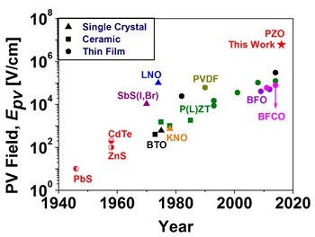
By contrast, there is another family of materials where photovoltages much larger than the bandgap can be achieved; they are the so-called ferroelectrics, intrinsically polar materials where the photovoltage is originated by the asymmetry of the crystal lattice instead of by a semiconductor interfacial effect. Until now, ferroelectric materials held the record for the highest photoelectric fields ever produced (the photovoltaic field is, in first approximation, the photovoltage divided by the thickness of the device).
Now, a multidisciplinary research team from the Institut Català de Nanociència i Nanotecnologia (ICN2), funded by Severo Ochoa Excellence Program, has reported in Advanced Materials the largest ever photovoltaic field, reaching values in excess of a million volt per centimetre and beating by a factor of x20 the previous state of the art. Furthermore they have discovered the effect in a class of materials (known as antiferroelectrics) where the photovoltaic effect had not been explored before. The ICN2 research team behind the discovery is formed by Dr Amador Pérez-Tomás from ICN2, Prof Mónica Lira-Cantú from CSIC and ICREA research professor Gustau Catalán.
It was in many ways a real surprise as these materials are antipolar and not polar (hence the name antiferroelectrics) and thus it was not expected to present stable photovoltaic action, but the authors have proposed an explanation for the observed results. There is, however, still some way for this discovery to be of practical use in photovoltaic cells, because even though their photovoltage is very large, their electrical current still remains too low, meaning that the electrical power is still below that of standard semiconductor devices. The researchers have nevertheless filled a patent to protect the technology, and are working on the optimization of the device to rapidly advance into practical applications as they believe it can find uses in practical applications such as photovoltaic sensors and photocatalysts.
Share on:


Testimonial
"Our marketing partnership with I-Connect007 is already delivering. Just a day after our press release went live, we received a direct inquiry about our updated products!"
Rachael Temple - AlltematedSuggested Items
Curing and Verification in PCB Shadow Areas
09/17/2025 | Doug Katze, DymaxDesign engineers know a simple truth that often complicates electronics manufacturing: Light doesn’t go around corners. In densely populated PCBs, adhesives and coatings often fail to fully cure in shadowed regions created by tall ICs, connectors, relays, and tight housings.
Marcy’s Musings: Advancing the Advanced Materials Discussion
09/17/2025 | Marcy LaRont -- Column: Marcy's MusingsAs the industry’s most trusted global source of original content about the electronics supply chain, we continually ask you about your concerns, what you care about, and what you most want to learn about. Your responses are insightful and valuable. Thank you for caring enough to provide useful feedback and engage in dialogue.
September 2025 PCB007 Magazine: The Future of Advanced Materials
09/16/2025 | I-Connect007 Editorial TeamMoore’s Law is no more, and the advanced material solutions being developed to grapple with this reality are surprising, stunning, and perhaps a bit daunting. Buckle up for a dive into advanced materials and a glimpse into the next chapters of electronics manufacturing.
I-Connect007 Launches Advanced Electronics Packaging Digest
09/15/2025 | I-Connect007I-Connect007 is pleased to announce the launch of Advanced Electronics Packaging Digest (AEPD), a new monthly digital newsletter dedicated to one of the most critical and rapidly evolving areas of electronics manufacturing: advanced packaging at the interconnect level.
Panasonic Industry will Double the Production Capacity of MEGTRON Multi-layer Circuit Board Materials Over the Next Five Years
09/15/2025 | Panasonic Industry Co., Ltd.Panasonic Industry Co., Ltd., a Panasonic Group company, announced plans for a major expansion of its global production capacity for MEGTRON multi-layer circuit board materials today. The company plans to double its production over the next five years to meet growing demand in the AI server and ICT infrastructure markets.