


 The Right Approach: The Pros and Cons of PCB Vertical Integration
 American Made Advocacy: PCBAA’s Fifth Annual Meeting—Growing Membership and Valuable Relationships
 It's Only Common Sense: Why the Best Years of Electronics Are Still Ahead of Us


Life has always played by its own set of molecular rules. From the biochemistry behind the first cells, evolution has constructed wonders like hard bone, rough bark and plant enzymes that harvest light to make food.
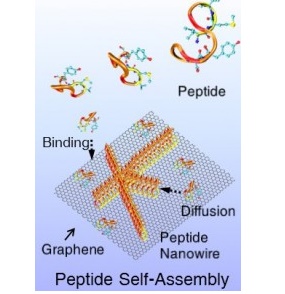
Depiction of peptides self-assembling into nanowires on a 2-D surface of the semimetal graphene. Mehmet Sarikaya
But our tools for manipulating life — to treat disease, repair damaged tissue and replace lost limbs — come from the nonliving realm: metals, plastics and the like. Though these save and preserve lives, our synthetic treatments are rooted in a chemical language ill-suited to our organic elegance. Implanted electrodes scar, wires overheat and our bodies struggle against ill-fitting pumps, pipes or valves.
A solution lies in bridging this gap where artificial meets biological — harnessing biological rules to exchange information between the biochemistry of our bodies and the chemistry of our devices. In a paper published Sept. 22 in Scientific Reports, engineers at the University of Washington unveiled peptides — small proteins which carry out countless essential tasks in our cells — that can provide just such a link.
The team, led by UW professor Mehmet Sarikaya in the Departments of Materials Science & Engineering, shows how a genetically engineered peptide can assemble into nanowires atop 2-D, solid surfaces that are just a single layer of atoms thick. These nanowire assemblages are critical because the peptides relay information across the bio/nano interface through molecular recognition — the same principles that underlie biochemical interactions such as an antibody binding to its specific antigen or protein binding to DNA.
Since this communication is two-way, with peptides understanding the “language” of technology and vice versa, their approach essentially enables a coherent bioelectronic interface.
“Bridging this divide would be the key to building the genetically engineered biomolecular solid-state devices of the future,” said Sarikaya, who is also a professor of chemical engineering and oral health sciences.
His team in the UW Genetically Engineered Materials Science and Engineering Center studies how to coopt the chemistry of life to synthesize materials with technologically significant physical, electronic and photonic properties. To Sarikaya, the biochemical “language” of life is a logical emulation.
“Nature must constantly make materials to do many of the same tasks we seek,” he said.
The UW team wants to find genetically engineered peptides with specific chemical and structural properties. They sought out a peptide that could interact with materials such as gold, titanium and even a mineral in bone and teeth. These could all form the basis of future biomedical and electro-optical devices. Their ideal peptide should also change the physical properties of synthetic materials and respond to that change. That way, it would transmit “information” from the synthetic material to other biomolecules — bridging the chemical divide between biology and technology.
In exploring the properties of 80 genetically selected peptides — which are not found in nature but have the same chemical components of all proteins — they discovered that one, GrBP5, showed promising interactions with the semimetal graphene. They then tested GrBP5’s interactions with several 2-D nanomaterials which, Sarikaya said, “could serve as the metals or semiconductors of the future.”
“We needed to know the specific molecular interactions between this peptide and these inorganic solid surfaces,” he added.
Their experiments revealed that GrBP5 spontaneously organized into ordered nanowire patterns on graphene. With a few mutations, GrBP5 also altered the electrical conductivity of a graphene-based device, the first step toward transmitting electrical information from graphene to cells via peptides.
In parallel, Sarikaya’s team modified GrBP5 to produce similar results on a semiconductor material — molybdenum disulfide — by converting a chemical signal to an optical signal. They also computationally predicted how different arrangements of GrBP5 nanowires would affect the electrical conduction or optical signal of each material, showing additional potential within GrBP5’s physical properties.
A top view image of GrBP5 nanowires on a 2-D surface of molybdenum disulfide.Mehmet Sarikaya/Scientific Reports
“In a way, we’re at the flood gates,” said Sarikaya. “Now we need to explore the basic properties of this bridge and how we can modify it to permit the flow of ‘information’ from electronic and photonic devices to biological systems.”
This is the focus of a new endeavor funded by the National Science Foundation’s Materials Genome Initiative. It will be led by Sarikaya and joined by UW professors Xiaodong Xu, René Overney and Valerie Daggett. Through UW’s CoMotion, he is also working with Amazon to cross that bio/nano divide for nano-sensors to detect early stages of pancreatic cancer.


