


 The Marketing Minute: Cracking the Code of Technical Marketing
 Trouble in Your Tank: Implementing Direct Metallization in Advanced Substrate Packaging


Enhancing the Superconducting Properties of an Iron-based Material
October 7, 2016 | BNLEstimated reading time: 4 minutes
Iron-based superconductors can conduct electricity without resistance at unusually high temperatures relative to those of conventional superconductors, which must be chilled to near absolute zero (minus 459 degrees Fahrenheit) to release their superconducting powers. In addition, they're relatively easy to bend and can carry electrical current easily in different directions under high magnetic fields before superconductivity becomes suppressed. These characteristics make iron-based superconductors promising for advanced energy applications, from electric vehicles to wind turbines and medical imaging devices. However, the amount of current they can carry has been low in comparison to other superconductors. Scientists have been trying to increase this amount, but doing so has often come at the cost of degrading another key superconducting property--the critical temperature at which superconductivity emerges.
Now, a team of scientists has come up with a way to double the amount of electrical current an iron-based material can carry without losing its superconducting properties, while increasing the material's critical temperature. Their method, reported in a paper published today in Nature Communications ("A route for a strong increase of critical current in nanostrained iron-based superconductors"), makes use of a readily available technology that could be used to improve the performance of superconducting wires and tapes.
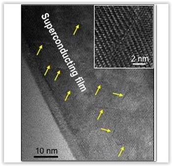
Superconducting Iron-Based Film
An electron microscope image of one of the team's superconducting iron-based films is shown after the scientists irradiated the film with low-energy protons shows the resulting chains of defects (indicated by yellow arrows). The inset image shows a zoomed-in view of a typical defect chain. (Image: Courtesy of the researchers)
"By bombarding the material with protons at low energy, we simultaneously increased the material's current-carrying capacity and critical temperature--the first time that this has been possible in an iron-based superconductor," said physicist Qiang Li, head of the Advanced Energy Materials Group at the U.S. Department of Energy's (DOE) Brookhaven National Laboratory, who directed the research. "There are low-energy ion facilities all over the world that can do this inexpensively."
Shooting ions at superconducting materials is a well-established method for artificially introducing defects in the crystal structure or chemistry of the materials to increase the amount of current they can carry. These defects "pin" in place, or trap, the microscopic magnetic vortices that form when the superconductor is placed in a strong magnetic field, such as those generated by magnets in magnetic resonance imaging (MRI) machines. If free to move around, the vortices dissipate energy, thereby destroying the superconductor's ability to carry electrical current without energy loss.
Unfortunately, if the defects produced by ion irradiation create too much disorder in the superconductor, they lower its critical temperature. Because superconductors currently require extreme cooling to conduct electricity without resistance, any decrease in the critical temperature is undesirable.
In a Goldilocks sense, the defects must be "just right"--not too big, not too small. Scientists can design such defects by selecting the appropriate ion species (e.g., protons, gold ions, argon ions) and ion energy.
"Some ions or energies may cause large enough damage to interfere with superconductivity, while others may not produce any effect at all," explained coauthor Toshinori Ozaki, a former scientist in Brookhaven Lab's Advanced Energy Materials Group who is now a faculty member at Japan's Kwansei Gakuin University. "So we run simulations to figure out what combination should produce the optimal defect--one that can hold down the magnetic vortices without negatively impacting the material's superconducting properties."
In the case of the iron-based material the team studied, low-energy protons did the trick. Using electron microscopes, the scientists took images of the thin films (about 100 nanometers thick) of the material they prepared, before and after they hit the films with low-energy protons.
"Throughout the irradiated films, we saw individual chains of defects created by the collisions between the incident ions and nucleus that broke the perfect atomic order, causing the lattice to locally compress or stretch out," said coauthor Lijun Wu, a materials scientist at Brookhaven who led the microscopy work.
In a performance check, the scientists measured the amount of electrical current running through the films in low and high magnetic fields. In high fields, the irradiated films carried more current than any low-temperature superconductor. This result suggests that the defects and local lattice strain must be strongly pinning the magnetic vortices that would otherwise impede the flow of current.
To figure out what caused the surprising increase in the critical temperature, the team created a strain "map" that laid out where the locally compressed and tensile (stretched out) regions were located. Previous studies had already shown that the type of lattice strain correlates with the critical temperature: highly compressed regions with a high critical temperature, and highly tensile regions with a low critical temperature. In the team's films, the compressive ones took up much more space, leading to an overall raised critical temperature.
According to Li, these performance gains are only the beginning: "We believe that the critical current and temperature can be further enhanced by fine tuning the structure of the defects and the arrangement of the lattice strains."
Share on:


Testimonial
"In a year when every marketing dollar mattered, I chose to keep I-Connect007 in our 2025 plan. Their commitment to high-quality, insightful content aligns with Koh Young’s values and helps readers navigate a changing industry. "
Brent Fischthal - Koh YoungSuggested Items
Curing and Verification in PCB Shadow Areas
09/17/2025 | Doug Katze, DymaxDesign engineers know a simple truth that often complicates electronics manufacturing: Light doesn’t go around corners. In densely populated PCBs, adhesives and coatings often fail to fully cure in shadowed regions created by tall ICs, connectors, relays, and tight housings.
Marcy’s Musings: Advancing the Advanced Materials Discussion
09/17/2025 | Marcy LaRont -- Column: Marcy's MusingsAs the industry’s most trusted global source of original content about the electronics supply chain, we continually ask you about your concerns, what you care about, and what you most want to learn about. Your responses are insightful and valuable. Thank you for caring enough to provide useful feedback and engage in dialogue.
September 2025 PCB007 Magazine: The Future of Advanced Materials
09/16/2025 | I-Connect007 Editorial TeamMoore’s Law is no more, and the advanced material solutions being developed to grapple with this reality are surprising, stunning, and perhaps a bit daunting. Buckle up for a dive into advanced materials and a glimpse into the next chapters of electronics manufacturing.
I-Connect007 Launches Advanced Electronics Packaging Digest
09/15/2025 | I-Connect007I-Connect007 is pleased to announce the launch of Advanced Electronics Packaging Digest (AEPD), a new monthly digital newsletter dedicated to one of the most critical and rapidly evolving areas of electronics manufacturing: advanced packaging at the interconnect level.
Panasonic Industry will Double the Production Capacity of MEGTRON Multi-layer Circuit Board Materials Over the Next Five Years
09/15/2025 | Panasonic Industry Co., Ltd.Panasonic Industry Co., Ltd., a Panasonic Group company, announced plans for a major expansion of its global production capacity for MEGTRON multi-layer circuit board materials today. The company plans to double its production over the next five years to meet growing demand in the AI server and ICT infrastructure markets.