


 The Marketing Minute: Cracking the Code of Technical Marketing
 Trouble in Your Tank: Implementing Direct Metallization in Advanced Substrate Packaging


New Advances in Solar Cell Technology
October 10, 2016 | OISTEstimated reading time: 4 minutes
With the high environmental cost of conventional energy sources and the finite supply of fossil fuels, the importance of renewable energy sources has become much more apparent in recent years. However, efficiently harnessing solar energy for human use has been a difficult task. While silicon-based solar cells can be used to capture sunlight energy, they are costly to produce on an industrial scale. Research from the Energy Materials and Surface Sciences Unit at the Okinawa Institute of Science and Technology Graduate University (OIST), led by Prof. Yabing Qi, has focused on using organo-metal halide perovskite films in solar cells. These perovskite films are highly crystalline materials that can be formed by a large number of different chemical combinations and can be deposited at low cost. Recent publications from Prof. Qi’s lab cover three different areas of innovation in perovskite film research: a novel post annealing treatment to increase perovskite efficiency and stability, a discovery of the decomposition products of a specific perovskite, and a new means of producing perovskites that maintains solar efficiency when scaled up.
In order to be useful as solar cells, perovskite films must be able to harvest solar energy at a high efficiency that is cost-effective, be relatively easy to manufacture, and be able to withstand the outdoor environment over a long period of time. Dr. Yan Jiang in Prof. Qi’s lab has recently published research in Materials Horizons that may help increase the solar efficiency of the organo-metal halide perovskite MAPbI3. He discovered that the use of a methylamine solution during post-annealing led to a decrease in problems associated with grain boundaries. Grain boundaries manifest as gaps between crystalline domains and can lead to unwanted charge recombination. This is a common occurrence in perovskite films and can reduce their efficiency, making the improvement of grain boundary issues essential to maintain high device performance. Dr. Jiang’s novel post annealing treatment produced solar cells that had fused grain boundaries, reduced charge recombination, and displayed an outstanding conversion efficiency of 18.4%. His treated perovskite films also exhibited exceptional stability and reproducibility, making his method useful for industrial production of solar cells.
Comparison of grain boundaries in MAPbI3 perovskite films following thermal annealing (a), DMF solvent annealing (b), and methylamine post annealing treatment. The methylamine post annealing treatment shows the most improvement, as the grain boundaries become fused and less defined after application.
One of the biggest disadvantages to the use of perovskites when compared to silicon in solar cells is their relatively short lifespan. In order to create a solar cell that can withstand the outdoor environment over a long period of time, it is crucial to determine the major products of perovskite decomposition. Previous research on MAPbI3 perovskite films led to the conclusion that the gas products of thermal degradation of this material were methylamine (CH3NH2) and hydrogen iodide (HI). However, exciting new research from Dr. Emilio J. Juarez-Perez, also in Prof. Qi’s lab, published in Energy & Environmental Science, shows that major gas products of degradation are methyliodide (CH3I) and ammonia (NH3) instead. Dr. Juarez-Perez used a combination of thermal gravimetric differential thermal analysis (TG-DTA) and mass spectrometry (MS) to correctly determine both the mass loss and chemical nature of these products. Because the products of decomposition have now been correctly identified, researchers can look for ways to prevent degradation of the material, leading to more stable materials for use in the future.
MAPbI3 perovskite films decompose to form methyliodide (CH3I) and ammonia (NH3), determined by thermal gravimetric differential thermal analysis and mass spectrometry
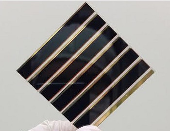
A pervasive problem in academic research is often the inability to scale up experiments for use in industry. While perovskite films can be made with relative ease on a small scale in the laboratory, they can be difficult to replicate on the large scale needed for mass production. New research from Dr. Matthew Leyden in the Journal of Materials Chemistry A has the potential to make industrial production of perovskites much easier. His work uses chemical vapor deposition, a cost-effective process commonly used in industry, to create large solar cells and modules of FAPbI3 perovskites. This is one of the first demonstrations of perovskite solar cells and modules fabricated by a method widely employed in industry, making the mass production of perovskite films more feasible. The solar cells and modules produced are significantly larger, e.g., 12 cm2, than those commonly studied in academia, typically <0.3cm2. These solar modules show enhanced thermal stability and relatively high efficiencies, which is impressive as many perovskite solar cells lose efficiency drastically as they are scaled up, making this type of research useful for commercial purposes.
Top photo depicts how perovskite films are made using the chemical vapor deposition (CVD) technique. Bottom left shows a perovskite solar module produced using the CVD technique. Bottom right displays the OIST logo made from perovskite using the same technique.
Research from Prof. Qi’s research unit has brought perovskite solar cells one step closer to mass production by providing solutions to problems of efficiency, life-span, and scalability. With more exciting research on the horizon, the unit is bringing the dream of utilizing cost-effective renewable energy resources into reality.
Share on:


Testimonial
"Advertising in PCB007 Magazine has been a great way to showcase our bare board testers to the right audience. The I-Connect007 team makes the process smooth and professional. We’re proud to be featured in such a trusted publication."
Klaus Koziol - atgSuggested Items
AI-Powered Wearables Transform How Consumers Interact with Everyday Technology
09/15/2025 | PR NewswireThe global demand for AI-driven, touchless wearable technologies is accelerating as consumers seek more natural, seamless and intuitive ways to interact with their devices. Traditional touch screens and voice assistants, while effective, are increasingly viewed as limiting in a world where multitasking, mobility and efficiency are key. As industries from consumer electronics to augmented reality and enterprise computing embrace the possibilities of gesture-based control, the market for neural interfaces is rapidly expanding
Kopin Announces $9 Million Follow-On Contract for Defense Thermal Imaging Assembly
08/14/2025 | BUSINESS WIREKopin Corporation, a leading provider of application-specific optical systems and high-performance microdisplays for defense, training, industrial, consumer and medical products, today announced the award of an approximate $9 million follow-on production contract in support of a custom thermal imaging assembly build for a major U.S. defense prime contractor.
Mouser Electronics Receives Top Global Distributor, Growth Awards from HARTING
08/01/2025 | Mouser ElectronicsMouser Electronics, Inc., the authorized global distributor with the newest electronic components and industrial automation products, has been honored with HARTING's prestigious Global High Service Distributor of the Year Award. Mouser also received the Distinguished Award for New Product Sales Growth. The awards were presented at HARTING's recent 2025 Distribution Summit in Louisville, Kentucky.
DigiKey Expands Inventory with Over 32,000 Stocking NPIs in Q2 2025
07/31/2025 | Digi-KeyDigiKey, the leading global electronic components and automation products distributor, extensively expanded its in-stock products available for same-day shipment by adding more than 32,000 innovative new product introductions (NPIs) in the second quarter of 2025.
It’s Only Common Sense: Selling to Today's Generation of Buyers
06/30/2025 | Dan Beaulieu -- Column: It's Only Common SenseMillennials and Gen Z hold significant purchasing power and influence in industries worldwide. Selling to them requires adapting to their unique preferences, behaviors, and values, and exploring their buying habits, embracing their emphasis on social values, and mastering digital communication. Unlike previous generations, they prioritize experiences, sustainability, and value.