


 The Marketing Minute: Cracking the Code of Technical Marketing
 Trouble in Your Tank: Implementing Direct Metallization in Advanced Substrate Packaging


Ultra-thin Ferroelectric Material for Next-generation Electronics
October 12, 2016 | Tokyo Institute of TechnologyEstimated reading time: 2 minutes
Scientists at Tokyo Institute of Technology have demonstrated the potential of a new, thin-film ferroelectric material that could improve the performance of next-generation sensors and semi-conductors (Scientific Reports, "The demonstration of significant ferroelectricity in epitaxial Y-doped HfO2 film").
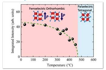
Integrated intensity of YHO-7 110 diffraction peak as a function of temperature. (Image: Tokyo Tech)
‘Ferroelectric’ materials can switch between different states of electrical polarization in response to an external electric field. This flexibility means they show promise for many applications, for example in electronic devices and computer memory. Current ferroelectric materials are highly valued for their thermal and chemical stability and rapid electro-mechanical responses, but creating a material that is scalable down to the tiny sizes needed for technologies like silicon-based semiconductors (Si-based CMOS) has proven challenging.
Now, Hiroshi Funakubo and co-workers at the Tokyo Institute of Technology, in collaboration with researchers across Japan, have conducted experiments to determine the ferroelectric properties of an inorganic compound called hafnium oxide (HfO2) for the first time. Crucially, the crystal structure of HfO2 allows it to be deposited in ultra-thin films, meaning it may prove invaluable for next-generation technologies.
Ferroelectric properties stem from the shape and structure of the crystal used. The team knew that an ‘orthorhombic’ crystal of HfO2 would likely exhibit ferroelectricity. Funakubo’s team wanted to pinpoint the material’s spontaneous polarization and the Curie temperature (the point above which a material stops being ferroelectric due crystal re-structuring). To do this, they needed to grow a carefully-ordered crystal on a substrate, a process known as epitaxy, which would give them well-defined data on an atomic scale.
The researchers found that one particular epitaxial film, labelled YHO-7, exhibited ferroelectricity with a spontaneous polarization of 45 µC/cm and a Curie temperature of 450 °C (see image). The experimental results confirm earlier predictions using first principle calculations.
From a scientific and industrial point of view, a Curie temperature of 450 °C is of great interest, because it means the material could fulfil functions for future technologies. In contrast to many existing ferroelectric materials, the new thin-film exhibits compatibility with Si-based CMOS and is robust in miniature forms.
Ferroelectric materials
Ferroelectric materials differ from other materials because their polarization can be reversed by an external electric field being applied in the opposite direction to the existing polarization. This property stems from the materials’ specific crystal structure. Ferroelectric materials are highly valuable for next-generation electronics. While a number of ferroelectric materials are known to science and are already used in different applications, their crystal structure does not allow them to be scaled down to a small enough, ultra-thin film for use in miniaturized devices.
The material used by Funakubo and co-workers, hafnium oxide (HfO2), had previously been predicted to exhibit ferroelectric properties through first principle calculations. However, no research team had confirmed and examined these predictions through experiments. Funakubo’s team decided to measure the properties of the material when it was deposited in thin-film crystal form onto a substrate. The precise nature of the crystal structure enabled the researchers to pinpoint the material’s properties in full for the first time.
Their discovery of a particular epitaxial thin-film crystal of HfO2 that exhibits ferroelectricity below 450 °C will be of great significance in the field.
Implications of the current study
Funakubo’s team are hopeful that their new thin film ferroelectric material will have applications in novel random-access memory and transistors, along with quantum computing. Their material is also the first ferroelectric material compatible with silicon-based semiconductors (Si-based CMOS).
Share on:


Testimonial
"The I-Connect007 team is outstanding—kind, responsive, and a true marketing partner. Their design team created fresh, eye-catching ads, and their editorial support polished our content to let our brand shine. Thank you all! "
Sweeney Ng - CEE PCBSuggested Items
Curing and Verification in PCB Shadow Areas
09/17/2025 | Doug Katze, DymaxDesign engineers know a simple truth that often complicates electronics manufacturing: Light doesn’t go around corners. In densely populated PCBs, adhesives and coatings often fail to fully cure in shadowed regions created by tall ICs, connectors, relays, and tight housings.
Marcy’s Musings: Advancing the Advanced Materials Discussion
09/17/2025 | Marcy LaRont -- Column: Marcy's MusingsAs the industry’s most trusted global source of original content about the electronics supply chain, we continually ask you about your concerns, what you care about, and what you most want to learn about. Your responses are insightful and valuable. Thank you for caring enough to provide useful feedback and engage in dialogue.
September 2025 PCB007 Magazine: The Future of Advanced Materials
09/16/2025 | I-Connect007 Editorial TeamMoore’s Law is no more, and the advanced material solutions being developed to grapple with this reality are surprising, stunning, and perhaps a bit daunting. Buckle up for a dive into advanced materials and a glimpse into the next chapters of electronics manufacturing.
I-Connect007 Launches Advanced Electronics Packaging Digest
09/15/2025 | I-Connect007I-Connect007 is pleased to announce the launch of Advanced Electronics Packaging Digest (AEPD), a new monthly digital newsletter dedicated to one of the most critical and rapidly evolving areas of electronics manufacturing: advanced packaging at the interconnect level.
Panasonic Industry will Double the Production Capacity of MEGTRON Multi-layer Circuit Board Materials Over the Next Five Years
09/15/2025 | Panasonic Industry Co., Ltd.Panasonic Industry Co., Ltd., a Panasonic Group company, announced plans for a major expansion of its global production capacity for MEGTRON multi-layer circuit board materials today. The company plans to double its production over the next five years to meet growing demand in the AI server and ICT infrastructure markets.