


 The Marketing Minute: Cracking the Code of Technical Marketing
 Trouble in Your Tank: Implementing Direct Metallization in Advanced Substrate Packaging


2D-nanocellulose: Piezoelectric Driven by a Hydrogen Bonds Pattern
October 12, 2016 | ICN2Estimated reading time: 1 minute
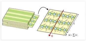
Researchers from ICN2 Phononic and Photonic Nanostructures Group publish in Scientific Reports findings providing the basis for new electromechanical designs using 2D-nanocellulose. In a longer-term perspective, the reinterpretation of electrical features for hydrogen bonds here introduced could pave the way in the understanding of life-essential molecules and events.
In the next coming years nanocellulose (NC) would attract lot of attention from industrial researchers (market value is estimated to be 530 M$ worldwide by 2020). The process of development and functionalization of NC materials is being promising because of their well-known unique optomechanical features and green nature. However, there is still a niche for applications based on NC electric-response. In this scenario, the results published in Scientific Reports with the participation of ICN2 researchers, would set up foundations for new strategies intended to drive novel applications based on 2D-NC with a predicted piezoelectric-response ~ pm V-1. This result could rank NC at the level of currently used bulk piezoelectrics like α-quartz and most recent 2D materials like MoSe2 or doped graphene. The first author of the article is Dr Yamila García, and the last one ICREA Research prof. Dr Clivia M. Sotomayor-Torres, Group leader of the ICN2 Phononic and Photonic Nanostructures Group.
"We are too big". It is one of the main limitations to do nanotechnology as Richard Feynman pointed out in 1959. As a contribution in paving the way to overcome this restriction, it is introduced a theoretical framework for the investigation of electric field profiles with interatomic resolution and thus to understand the fundamentals of the electromechanical coupling at the nanoscale. Remarkably, the mean-field descriptor obtained with the methodology described in the manuscript would also complete the latest definition of hydrogen bonds stated by IUPAC since it is the first effective approach in quantifying the electrical nature of such interactions.
An "atom by atom" understanding of electrical forces managing directional bonds is needed if we plan to engineer materials by means of highly selected nanoscale oriented mechanisms. So then, deepening on the understanding of 2D-NC as a piezoelectric system managed by electroactive and well-distinguishable HB could facilitate new openings for nanotechnologies community intended to progress on NC applications, i.e. straightforwardly introducing electronic-base sensing and actuating applications. Looking to the future, areas like molecular biology or genetic engineering would be benefited by the new contributions on the understanding of electrical forces within life-essential hydrogen bonds.
Share on:


Testimonial
"Our marketing partnership with I-Connect007 is already delivering. Just a day after our press release went live, we received a direct inquiry about our updated products!"
Rachael Temple - AlltematedSuggested Items
Curing and Verification in PCB Shadow Areas
09/17/2025 | Doug Katze, DymaxDesign engineers know a simple truth that often complicates electronics manufacturing: Light doesn’t go around corners. In densely populated PCBs, adhesives and coatings often fail to fully cure in shadowed regions created by tall ICs, connectors, relays, and tight housings.
Marcy’s Musings: Advancing the Advanced Materials Discussion
09/17/2025 | Marcy LaRont -- Column: Marcy's MusingsAs the industry’s most trusted global source of original content about the electronics supply chain, we continually ask you about your concerns, what you care about, and what you most want to learn about. Your responses are insightful and valuable. Thank you for caring enough to provide useful feedback and engage in dialogue.
September 2025 PCB007 Magazine: The Future of Advanced Materials
09/16/2025 | I-Connect007 Editorial TeamMoore’s Law is no more, and the advanced material solutions being developed to grapple with this reality are surprising, stunning, and perhaps a bit daunting. Buckle up for a dive into advanced materials and a glimpse into the next chapters of electronics manufacturing.
I-Connect007 Launches Advanced Electronics Packaging Digest
09/15/2025 | I-Connect007I-Connect007 is pleased to announce the launch of Advanced Electronics Packaging Digest (AEPD), a new monthly digital newsletter dedicated to one of the most critical and rapidly evolving areas of electronics manufacturing: advanced packaging at the interconnect level.
Panasonic Industry will Double the Production Capacity of MEGTRON Multi-layer Circuit Board Materials Over the Next Five Years
09/15/2025 | Panasonic Industry Co., Ltd.Panasonic Industry Co., Ltd., a Panasonic Group company, announced plans for a major expansion of its global production capacity for MEGTRON multi-layer circuit board materials today. The company plans to double its production over the next five years to meet growing demand in the AI server and ICT infrastructure markets.